Via Stubs: Practical Strategies To Mitigate Return Loss
(This is the second in a series of blogs, from Sandeep Sankararaman, Samtec’s Principal RF and Signal Integrity Engineer, discussing design strategies for high-bandwidth RF launches. The first is entitled “What Is An RF Connector Launch?” The third is “Maximizing RF Launch Performance: The Impact of GND Vias.” coming next week, discusses GND rings.)
When using a through via to transition to an internal layer, there is a stub created by the part of the via that extends below the transition layer. The higher the bandwidth goal, the more this stub impacts the performance. The impact of the stub is the worst at a frequency where the stub length equals ¼ of the wavelength.
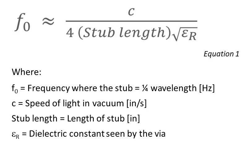
While f0 is the frequency at which the impact is most prominent, well before this frequency the via stub starts to degrade the performance of the via transition because it adds additional capacitance to the launch.
A common strategy used to minimize the impact of via stubs is to backdrill most of the stub away. In the backdrilling process, the PCB fabricator drills out the via stub from the side opposite the connector launch. However, there is always a residual stub left behind.
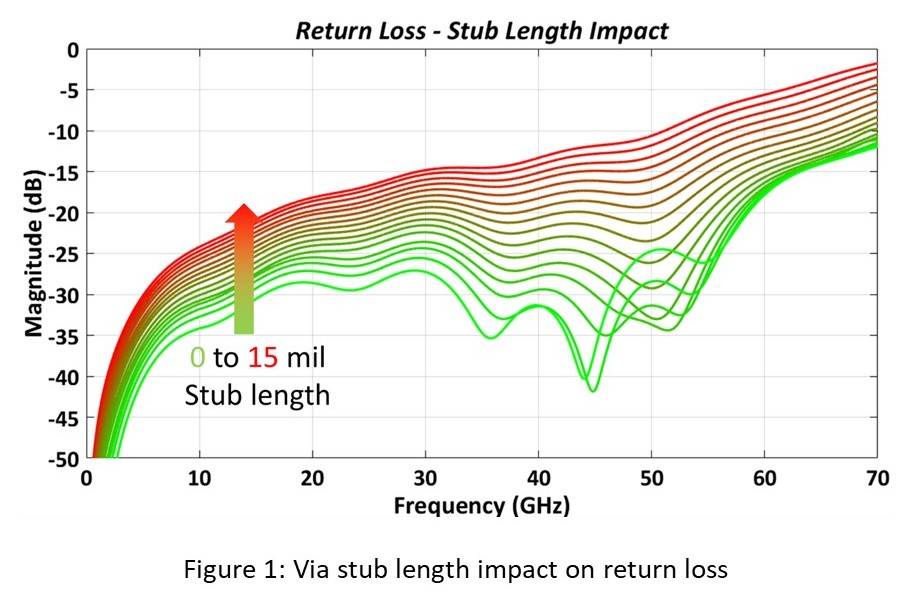
To illustrate the need to push for the smallest stub length, look at the curves shown in Figure 1. We see 16 curves in the graph, each one corresponding to a stub length between 0 and 15 mils. The smaller the stub length, the better the return loss across the frequency band.
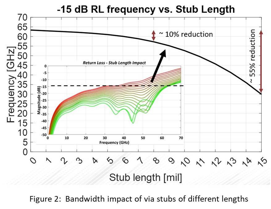
To better visualize the bandwidth impact, the frequency at which the return loss crosses the 15 dB level (VSWR = 1.4) is plotted in Figure 2. Notice two important points about the shape of the curve: (i) the curve is not linear, with longer stub lengths causing a rapid drop off in the bandwidth of the via transition, and (ii) for small stub lengths the reduction in bandwidth is not significant. Hence, pushing for a small residual stub and a tight tolerance provides a significant benefit not only from the point of view of increasing the operating bandwidth of the launch but also from the point of view of all launches on the board behaving similarly to one another.
Ideally, the best mitigation strategy against via stubs is to go with laser vias that do not have via stubs. If however, backdrilled vias must be used, it is possible to compensate for the capacitance introduced by the stub to a limited extent in the design of the launch.
In designing the compensation structure, it might be tempting to compensate for the worst-case stub length. This, however, can still result in poor performance, if the stub tolerance is large. To clarify this, look at Figure 3. Here a tolerance of 4 mils on the 6 mil nominal stub is assumed. The launch compensation is designed to provide the best impedance match for the worst-case stub length of 10 mils. Thus, for a 10 mil stub, the impedance of the launch is within 1 Ohm of nominal.
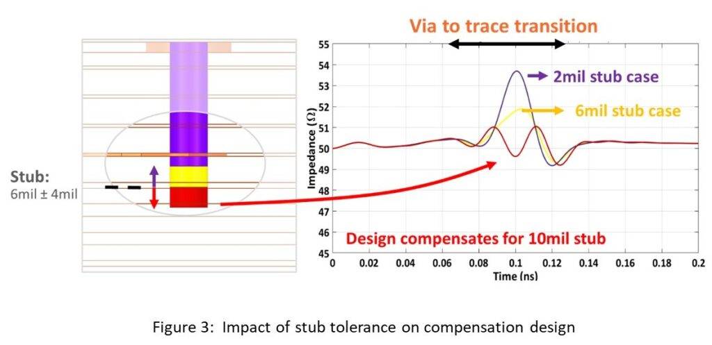
The problem arises for vias with the stub length at the other end of the tolerance (2 mils). For this stub length, the launch looks quite inductive. Keep in mind that all via stubs in the board need not have the same length. The ±4mil tolerance can result in some vias looking inductive and others not, perhaps even when they are adjacent launches.
To learn about how to design wide bandwidth connector launches please check out Wideband RF Launches: Literally Everything You Need To Know. And here’s a link if you want to learn about Samtec RF Products.