Maximizing RF Launch Performance: The Impact Of GND Vias
(This is the third in a series of blogs, from Sandeep Sankararaman, Samtec’s Principal RF and Signal Integrity Engineer, discussing design strategies for high-bandwidth RF launches. The first is entitled “What Is An RF Connector Launch?” The second is “Via Stubs: Practical Strategies To Mitigate Return Loss.“)
A wide bandwidth RF launch requires a good ground ring structure around the signal via to maintain the impedance while the signal travels down the via. Figure 1 shows the ground ring for a 90 GHz bandwidth launch. Details about the design of RF launches can be found in “Wideband RF Launches: Literally, Everything You Need To Know.”
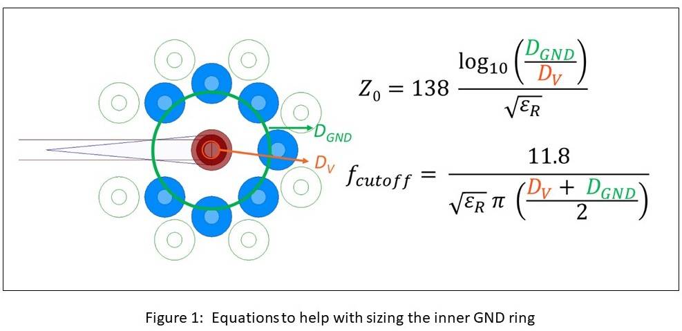
The via ground ring highlighted in blue in Figure 1, has a strong influence on the performance of the launch. There are two main factors that determine the diameter of the inner GND via ring:
The Impedance of the Launch Area
Figure 1 shows that the impedance of the launch area can be determined, to the first order, by treating the signal drill size as the center conductor diameter of a coax and the inner GND ring diameter as the shield diameter of a coax. For long vias, the nominal system impedance (e.g.: 50 Ohms) can be used as the target impedance. Short vias, however, are strongly impacted by the capacitive loading caused by the interaction between the launch and the end of the connector body. For this reason, a higher target Z0, like 70 Ohms, is better. That way the average effect of the connector + launch via is closer to 50 Ohms.
The Cutoff Frequency of the Higher Order Modes Supported by the Launch
Normally, in a launch for a coaxial RF connector, we want only the fundamental mode to propagate. This is the transverse electromagnetic mode (TEM). Above a certain frequency, called the cutoff frequency, the launch can support higher order modes. When this happens, energy is spread among the different modes and since the different modes propagate differently, the signal gets distorted quickly. To prevent this, the launch needs to be designed so the cutoff frequency lies outside the bandwidth of interest. Figure 1 shows that the cutoff frequency is inversely proportional to both the size of the GND ring and the dielectric constant seen when traveling down the via. The higher these numbers are, the lower the cutoff frequency and the lower the operating bandwidth of the launch. The formula for fcutoff in Figure 1 provides the cutoff frequency in GHz when the diameters (Dv, DGND) are given in inches.
Both the impedance and the cutoff frequency are also inversely proportional to the dielectric constant (eR) seen by the signal as it travels down the via. It is important to note that this eR need not match the value seen by the trace. The reason is PCBs are comprised of laminates bonded together. The laminates are composites and consist of glass fiber and resin.
Figure 2 shows a cross-sectional picture of a PCB. There are both core layers and pre-preg layers, each consisting of layers of glass cloth and resin. Since each of these layers has different dielectric properties, the effective dielectric constant seen by the signal depends on the direction in which it is traveling. PCBs in other words are anisotropic as far as the dielectric constant is concerned. The higher the anisotropy, the greater the difference in dielectric constant seen by the via as compared to the trace.
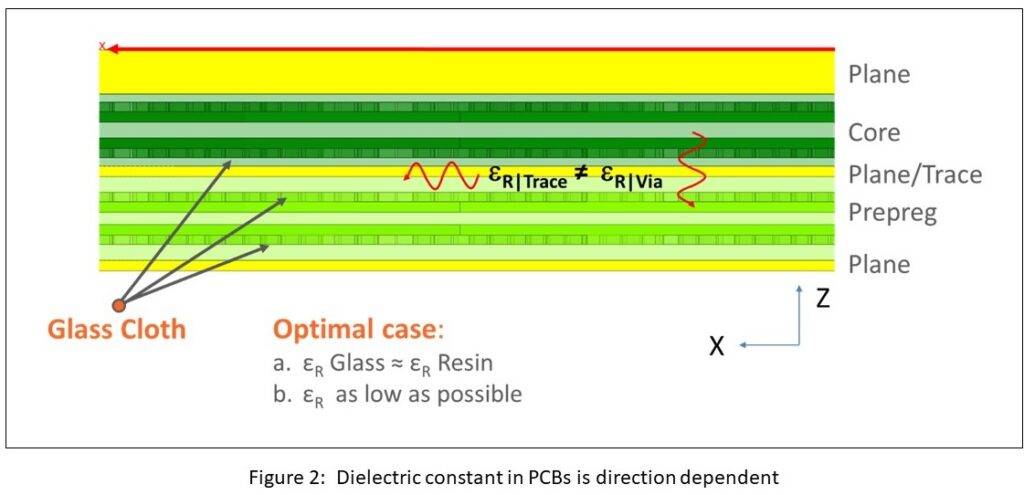
To achieve high bandwidth launches, the dielectric constant of both the resin and the glass should be low and equal. This ensures the lowest possible dielectric constant around the via and therefore, the highest cutoff frequency. The table in Figure 3 shows that to reach cutoff frequencies of >90 GHz, signal drill diameters of <5mils and dielectric constants of <3.1 are needed. The values in Figure 3 can serve as a useful starting point in guiding the design of an RF launch.
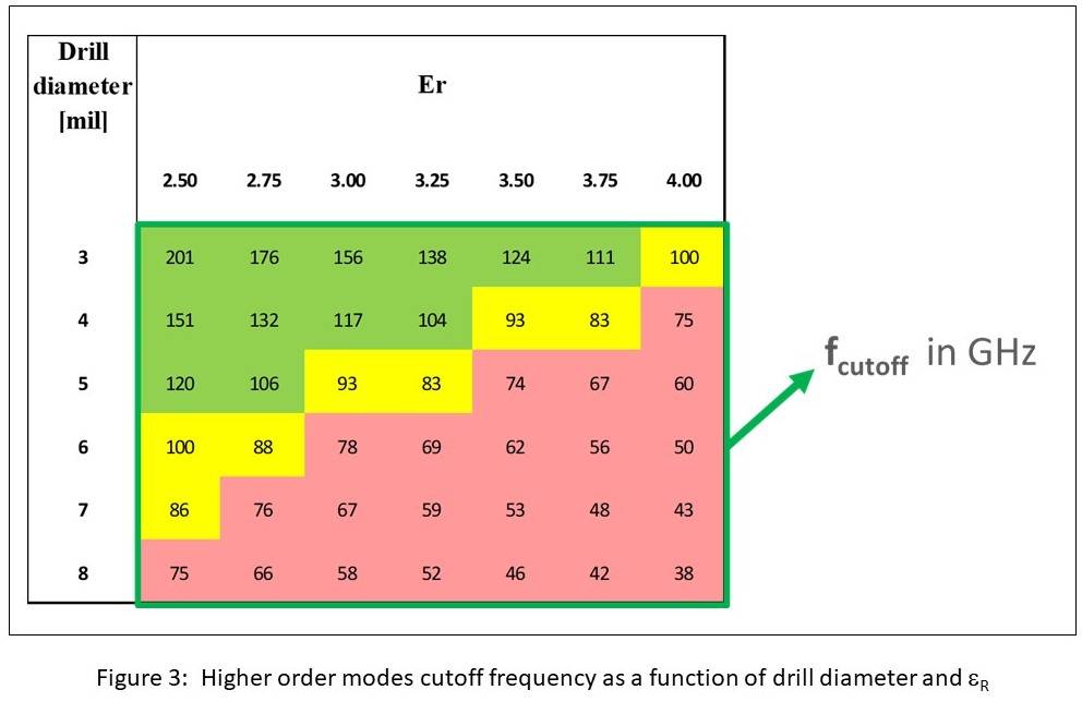
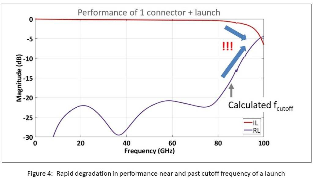
From Figure 3 it is possible to understand mathematically why the launch performance quickly degrades around the cutoff frequency, as seen in Figure 4. To get a physical explanation of what is happening, refer to Figure 5. Here the physical structure of the launch via and the surrounding GND vias is shown on the left side of the figure. The portion of the vias colored in green represents the portion that we want the signal energy to travel in. However, since the GND vias are through vias, they continue below the reference layer of the trace to form waveguide structures below the signal reference layers. To better visualize this, a conceptual schematic is shown on the right half of Figure 5.
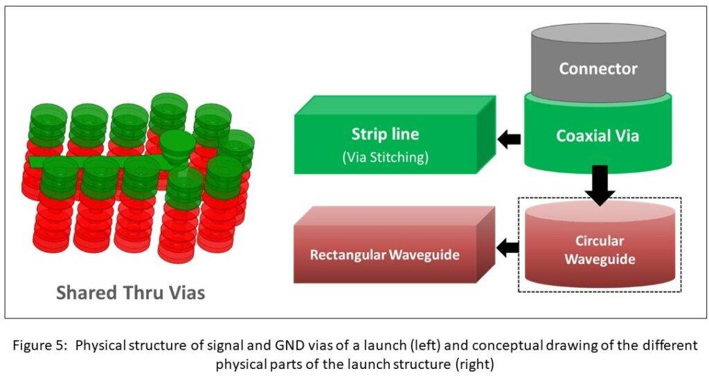
The right half of Figure 5 shows that the connector launches the energy into the coaxial portion of the launch and then the signal energy propagates down a stripline. However, below the trace reference layer, the GND vias form a circular waveguide under the signal via. There are also several rectangular vias formed by the plane layers and stitching GND vias under the trace reference layer. The circular waveguide and rectangular waveguides under the trace are non-TEM structures. That means they cannot propagate energy below fcutoff.
With this understanding, let us look at how energy flows in the launch at different frequencies. Figure 6 shows the electric field patterns in the launch below fcutoff (on the left) and above fcutoff (on the right). Below fcutoff, the energy stays contained within the stripline layers, and the circular waveguide below the signal via cannot propagate energy. This is exactly what we want to happen.
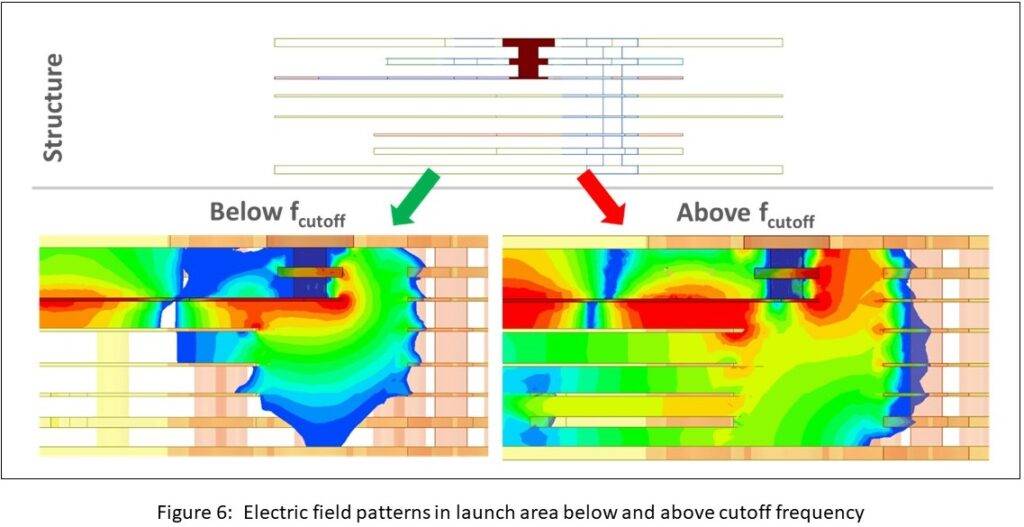
Above fcutoff though, the circular waveguide can now propagate energy and remove energy from the TEM mode traveling down the stripline and sends a portion of it through the rectangular cavities below the trace reference layer.
This is an undesirable situation because the energy can spread through the plane cavities to other parts of the board and cause crosstalk, radiation, and other undesirable effects. Staying below fcutoff, therefore, has the utmost importance in obtaining a high performance, wide bandwidth launch. An animation of the field plots is available here.
Here’s a link to see all of Samtec’s RF connector products.