Wideband RF Launches: Literally, Everything You Need To Know
As the demand for higher frequencies and wider bandwidths continue their relentless march upward, RF connectors need to keep up and even exceed this demand. Mating the RF connector to a PCB or substrate requires careful consideration of several factors to get the full performance out of the connector.
Let’s frame this concept by starting with a simple analogy: Putting tractor tires on a race car is not a recipe for success.
Tires on a race car need to convert power from the engine into speed on the road, all while maintaining the appropriate level of traction. Too much traction and the car slows down, too little and it slips. Think of a high-performance, wide bandwidth RF connector as the race car. A well-designed launch is equivalent to having optimal tires that allow the race car to win!
Sandeep Sankararaman, Samtec’s Principal RF and Signal Integrity Engineer, has 20 years of experience in signal and power integrity for IC packages, PCBs, and connectors. In the article below, Sandeep explains the essential components of an RF launch and the knobs to turn to optimize its performance. He uses frequently asked questions (FAQs) to guide this discussion.
Following are the questions and topics. Click on any of these questions to take you directly to that section of the page.
- What is an RF launch?
- Is a PCB Footprint the same as an RF launch?
- Why does someone need to consider this entire structure when optimizing an RF launch?
- How do you de-embed the fixture?
- In that case, how do you get to a higher frequency?
- Where do you actually start when optimizing an RF launch?
- Where should a reference plane be placed in a 3D EM solver?
- Are there other components that need to be considered when optimizing the RF launch?
- Regarding a via: I understand the drill hole size is a key dimension. What other aspects of the via are critical when considering RF launch effects?
- We know to start with a 3D EM solver, to consider all sub-components within an RF launch, and how via selection impacts performance. What should the next area of focus be?
- Why is the choice of the signal drill size so critical?
- You mentioned “mode” above. What is a mode?
- The via impedance and cutoff frequency also seem to depend on the “Dielectric constant in the XY plane.” How is that different from the regular value of Er?
- How do you verify if the value from the sizing estimates is correct for any particular implementation?
- While extremely helpful, I understand E field animations are time and resource-intensive. Is there another tool that can be used?
What is an RF launch?
SANDEEP: In simple terms, the launch is the mating structure that couples the electromagnetic energy in the connector to the PCB.
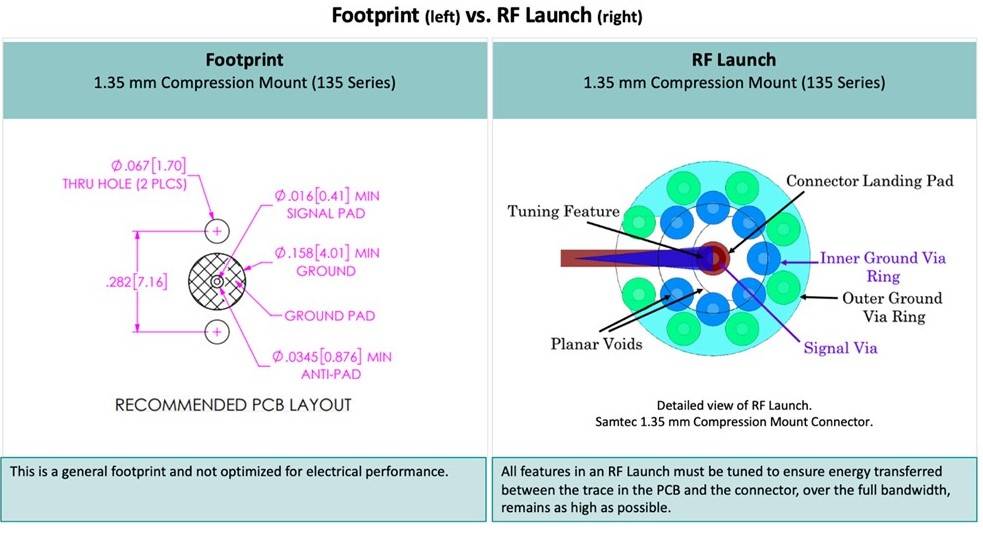
Is a PCB Footprint the same as an RF launch?
SANDEEP: No. Sometimes people think of the RF launch as just the footprint of the connector. However, simply instantiating a general footprint onto a PCB and expecting good performance is not likely to be successful. Instead, a high bandwidth launch has multiple features that, together with the connector, work to transfer the most amount of energy from the connector to the PCB trace. Let’s look at an example of this. The picture below is the footprint of a 1.35mm compression mount connector, while the picture on the right shows the optimized launch of the same connector.
Why does someone need to consider this entire structure when optimizing an RF launch?
SANDEEP: Having an optimized RF launch structure means the frequency can be pushed even higher, and in doing so, the DUT can be tested in a cleaner manner at those higher frequencies.
To understand this, we need to take a high-level view of the problem we are trying to solve. Let’s use a test application as our example, where the goal is to look at the true performance of the device being tested (DUT).
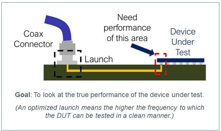
Ideally, we want to connect the test instrumentation to the solder balls of the device directly. This is not practical. Instead, the test cable, connector on the PCB, and the trace to the DUT are de-embedded from the measurement. This process mathematically removes the test fixturing and renders it electrically invisible when looking at the device’s performance.
How do you de-embed the fixture?
SANDEEP: One common way is to build a 2X thru structure on the same PCB as the DUT test board. As the name suggests, this structure consists of the test fixturing connected back-to-back. The figure below shows what this could look like.
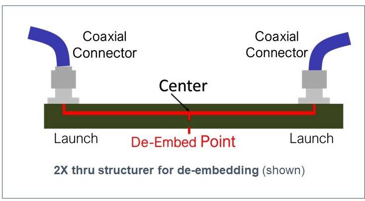
The de-embedding algorithm is able to use the measurement of the 2X thru structure to remove the effects of the test fixture up to a frequency where the separation between the IL and RL of the 2X thru is ≥ 5dB. And, as mentioned, the higher we can push this frequency, then the higher the frequency to which the DUT can be tested in a clean manner.
In that case, how would you get to a higher frequency?
SANDEEP: Getting to higher frequencies requires both minimizing the insertion loss and the return loss of the 2X thru structure. This can be done by tuning all of the features of the RF launch.
Where do you actually start when optimizing an RF launch?
SANDEEP: The starting point for launch optimization is done with the help of a 3D electromagnetic (EM) field solver, such as Ansys HFSS. Take a look at the figure below:
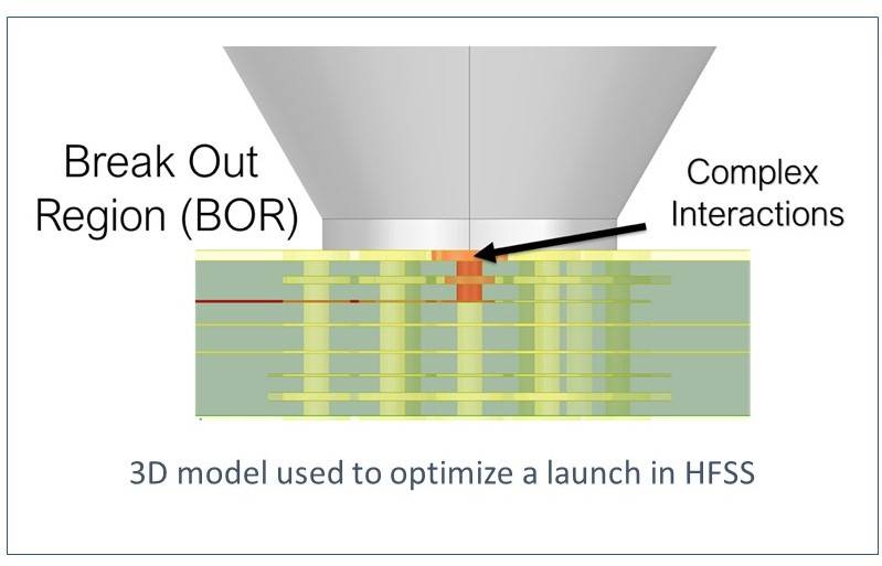
“Reference planes” are used at the ends of a 3D EM solver model to terminate it. The reference planes are areas of the model where the fields are well defined (such as TEM waves), which allows the fields to be solved accurately using 2-dimensional ports. In between the reference planes there are complex field interactions taking place because of the number of geometry changes.
Where should a reference plane be placed in a 3D EM solver?
SANDEEP: In the case of an RF connector launch, the fields a couple of mm inside the connector, when seen from the PCB interface, is a good location for a reference plane. Similarly, another reference plane can be placed on the trace a couple of mm after the launch via. This way the complete physics at the transition is captured and allows the S-parameters generated from the model to be cascaded with other pieces of the full path from the test instrument to the DUT.
Are there other components that need to be considered when optimizing the RF launch?
SANDEEP: Yes, absolutely. All sub-components of the launch should be considered, as these are the “knobs to turn” for complete optimization. These include the landing pad, signal via, tuning feature, planes, voids, ground collar, and ground rings.
Click here for details on RF launch sub-components.
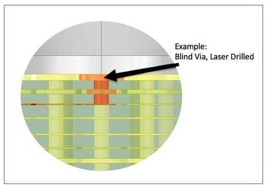
Regarding a via: I understand the drill hole size is a key dimension. What other aspects of the via are critical when considering RF launch effects?
SANDEEP: If the signal trace is not escaping on the top layer of the PCB, a via transition is needed. There are 2 options:
- a regular through via that goes all the way through the PCB
- a blind via that goes from the top layer to an internal routing layer only
The following shows an example of a blind via that is drilled using a laser.
There are advantages and disadvantages to each approach. Click here for details, such as the impact of via stubs.
We know to start with a 3D EM solver, to consider all sub-components within an RF launch, and how via selection impacts performance. What should the next area of focus be?
SANDEEP: Inner GND ring sizing and structure. The vias that make up the inner GND ring serve to carry the return current as the signal travels along the via. The GND via structure can be thought of as the shield of a coax cable. For this to be true the spacing between the GND vias should be less than ¼ of the wavelength at the maximum frequency of interest. Click here for details.
The equation (Equation 2) outlined in this detailed document shows that the inner GND sizing is heavily dependent on the drill size of the signal via. As we aim for higher bandwidths, the choice of the signal drill size is extremely critical.
Why is the choice of the signal drill size so critical?
SANDEEP: Let’s look at Eqn. 3 to understand why:
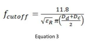
Equation 3 shows that there is a certain frequency (fcutoff) above which the signal can propagate in more than one mode simultaneously and that the fcutoff is inversely proportional to the signal drill size and inner GND ring size (this can be converted to a function of signal drill size using Equation 1).
Click here for more details.
Key takeaway: Think of using 6 mil drills and dielectrics with Er < 3 to get the really wide bandwidths.
You mentioned “mode” above. What is a mode?
SANDEEP: A mode is a particular field pattern that can propagate in the structure. In general, we want the signal to operate in the Transverse Electro-Magnetic mode (TEM), but above fcutoff , it is possible for other modes to also propagate in the structure. The higher-order modes will take energy away from the desired TEM mode. Different modes have different propagation characteristics, which means a signal propagating along different modes simultaneously is going to distort very quickly. Suppressing the generation and propagation of the higher-order modes ensures the signal quality for longer distances.
The via impedance and cutoff frequency also seem to depend on the “Dielectric constant in the XY plane.” How is that different from the regular value of Er?
SANDEEP: The dielectric constant for any material can be different along the X, Y, and Z axes. Commonly, we treat the dielectric constant the same in all directions. Materials exhibiting this behavior are called isotropic. This is not true for many PCB laminates, which are composite materials. They consist of glass fibers in a resin matrix. Resin and glass have different dielectric constants. As a result, the dielectric constant in the plane of the trace is different than the dielectric constant perpendicular to the plane of the trace (the dielectric constant around the via), making the material anisotropic [3].
Usually, the dielectric constant seen by the signal while traveling down the via is higher than the dielectric constant seen while traveling along the trace (Anisotropy > 1). To push the performance bandwidth, a lower Er is preferred, which implies a material with anisotropy close to 1 is preferred.
How do you verify if the value from the sizing estimates is correct for any particular implementation?
SANDEEP: To understand this let us look at how the energy flows when the GND ring is not properly sized. The structure below consists of a 90 GHz bandwidth connector mounted on a layer 1 to 3 laser via.
As you can observe from the E field animation examples, as long as the frequency is below the cutoff frequency, all the energy propagates down the stripline. If above the cutoff frequency then a significant amount of energy diverts into the PCB cavities.
While extremely helpful, I understand E field animations are time and resource-intensive. Is there another tool that can be used?
SANDEEP: Yes. Loss factor is another way of looking at the behavior of the inner GND ring. The loss factor is a measure of the energy that does not reach any of the ports of the structure but is instead dissipated through other means. The figure below shows the loss factor for the structure in the animations. It shows the power that is neither reflected to port 1 nor transmitted to port 2 – in other words, the energy that is going to couple to other structures and cause crosstalk and radiation issues.
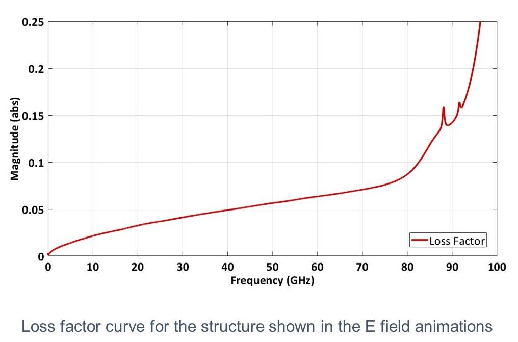
This shows that below approximately 80 GHz (for a 90 GHz bandwidth connector), the loss gradually increases. This corresponds to losses due to Cu and the dielectric. Above 80 GHz, the loss increases sharply. This is the sign that the structure is no longer behaving as designed. Making sure this knee frequency is outside the bandwidth of interest is key for a high-performance launch.
Can you provide insight into what is happening physically to cause the loss factor to change?
SANDEEP: Yes. Look at the figure below. The sections of the launch colored green indicate parts of the launch structure where we want the signal energy to flow.
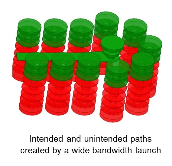
However, we are using through vias for the GND structure. That means the part of the GND vias below the trace area form additional structures that can carry signal energy under the proper conditions. To visualize the structures better, look at the conceptual diagram of the launch below.
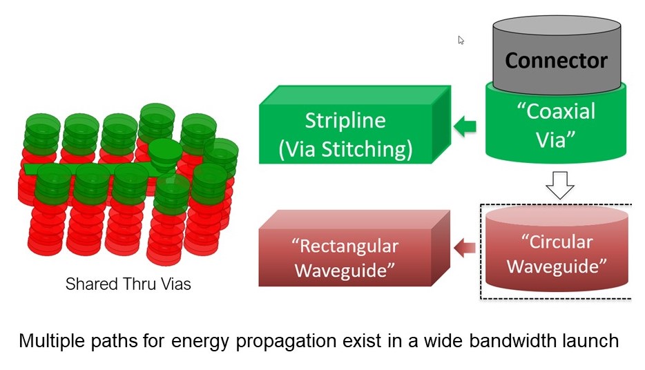
Right below the coaxial signal via lies a circular waveguide formed by the shared GND vias. Once the frequency increases past the cutoff frequency of the circular waveguide, it will allow energy to couple into all the rectangular waveguides created by the planes in the PCB that connect to the circular waveguide. For good performance, therefore, it is necessary to stay below the cutoff frequency of the coax via (Equation 3), which in turn is lower than the cutoff frequency of the circular waveguide.
To discuss your RF Launch and System Optimization requirements, please contact [email protected]
References:
1. S. Tucker, S. Sankararaman, T. Ellis, PCB Stackup & Launch Optimization in High-speed PCB Designs, DesignCon 2022
2. Quarter wavelength stub formula
3. S. McMorrow, E. Sayre, C. Nwachukwu, D. Blankenship, Anisotropic Design Considerations for 28 Gbps Via to Stripline Transitions, DesignCon2015.