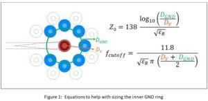
(This is the third in a series of blogs, from Sandeep Sankararaman, Samtec’s Principal RF and Signal Integrity Engineer, discussing design strategies for high-bandwidth RF launches. The first is entitled “What Is An RF Connector Launch?” The second is "Via Stubs: Practical Strategies To Mitigate Return Loss.") A wide bandwidth RF launch requires a good ground ring structure around the signal via to maintain the impedance while the signal travels down the via. Figure 1 shows the ground ring … [Read more...]
Making High Speed PCB Design Easier
High-speed PCB design for applications supporting data rates of 28 Gbps and beyond provides many challenges. PCB designers and layout engineers need to answer many questions: What PCB laminate offers the best performance? What connectors will be used? What is the stack up? How many layers? What about back drilling vias? There are a plethora of other variables that are beyond the scope of this blog. Fortunately for PCB designers and layout engineers, Samtec provides many … [Read more...]