Making High Speed PCB Design Easier
High-speed PCB design for applications supporting data rates of 28 Gbps and beyond provides many challenges. PCB designers and layout engineers need to answer many questions: What PCB laminate offers the best performance? What connectors will be used? What is the stack up? How many layers? What about back drilling vias?
There are a plethora of other variables that are beyond the scope of this blog. Fortunately for PCB designers and layout engineers, Samtec provides many tools to ease the PCB design process once the connector selection has been made.
Recommended PCB Layouts
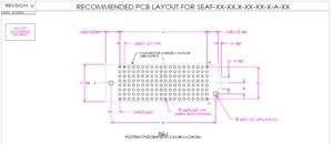
The Samtec customer support teams receive consistent requests for recommended PCB layouts of standard Samtec connectors. These critical dimensions are communicated via online drawings, which are available for virtually every Samtec connector.
Here is an example of the Recommended PCB Layout for the SEAF series. PCB designers use this as a guide for developing the appropriate PCB footprint.
PCB Footprints
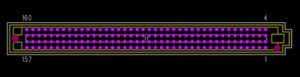
PCB designers manually transfer the Recommended PCB Layout into a digital footprint, then into a PCB design tool. This process can be tedious and time-consuming. The slightest error can lead to major headaches during PCB manufacturing.
Samtec has developed a number of digital PCB footprints where this critical translation is already completed. The resulting footprint files are checked against a known connector print eliminating errors for the PCB designer.
Samtec’s PCB footprints are available in several popular software packages, including but not limited to:
- Allegro V15.5 (and later)
- Altium Designer
- ASCII
- Eagle
- Mentor Expedition
- Mentor PADs
- OrCAD® .MAX
- OrCAD® Layout
Technical support for all PCB footprints is available via [email protected].
PCB CAD Libraries
In addition to footprints, PCB designers often create schematic symbols that link to the specific footprint. Samtec has created numerous PCB CAD libraries that speed up design flow and enable schematic circuit checking, bill of material generation, and automated board test and simulation. Dynamic linking of footprint and schematic data allows changes in either to be made and compared on the fly.
Samtec’s full connector PCB CAD libraries feature a complete part file incorporating footprint, schematic symbol, attributes, pin and gate mapping/swapping, and alphanumeric pin names in a PADs format. Samtec’s PCB CAD libraries enable accurate connector pad, hole, and mounting feature dimensions and locations.
Technical support for all PCB CAD libraries is available via [email protected].
Samtec Breakout Regions (BORs)
One of the largest challenges PCB designers face is developing BORs to optimize the performance of their PCBs. BORs are the area on the PCB where traces are “broken out” as required to attach the connector terminals to the PCB. If not done correctly, system performance can suffer.
Samtec has engineered connector pin transitions for optimized PCB performance in conjunction with the connector performance. It is highly recommended to utilize these guidelines to ensure the highest performance possible.
Under NDA, Samtec can provide PCB designers with the BOR PCB physical artwork and electrical models (S-parameters, etc.). Samtec BORs offer simplified PCB design and tested and verified solutions from across the Samtec connector portfolio.
Technical support for all BORs is available via [email protected].
Samtec 2D/3D Model Configurator
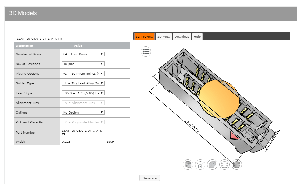
PCB designers may work with mechanical engineers to model the entire system in an MCAD environment. Samtec has developed their 3D Model Configurator to allow engineers to dynamically configure, preview, and download connector models from across the Samtec portfolio.
2D/3D connector models are available in over 150 native formats including:
- AutoCad
- Solid Edge
- Inventor3D Studio Max
- 3D Studio Max
This new tool helps PCB designers improve speed and accuracy in their projects. It also provides flexibility to port models from tool-to-tool.
Samtec customers continue to adopt this tool. On average, Samtec has approximately 1,000 downloads a day from the 3D Model Configurator. New models can be added in 24 hours.
Technical support for all PCB footprints is available via [email protected].