Samtec Flyover Minimizes Signal Loss
Martin Rowe and our friends at EDN recently ran an article entitled “High-Speed Signals Jump Over PCB Traces.” Martin begins by explaining that every time serial data rates increase, they expose problems masked at slower speeds. He goes on to summarize, “Many of those problems occur because of decreased signal integrity from losses that occur in PCB traces, vias, and connectors … Boards used in servers and switches are often quite large and they typically have “out of the box” I/O (copper or fiber) on one end and a backplane connection on the other.
To minimize the overall distance that a signal travels, PCB designers will place the switching IC (FPGAs or ASICs) in roughly the center of the board. Sure, you can minimize signal losses between the outside I/O and the switch devices by placing them close together, but that only worsens signal integrity from the ASIC or FPGA to the backplane.”
He points out that “To help with signal losses at 56 Gbits/s, many engineers are moving to 4-level pulse-amplitude modulation (PAM4), which doubles the data rate for a given signaling rate versus NRZ. Thus, a 14-GHz clock can deliver 56 Gbits/s using PAM4, but there’s a problem. The signal amplitude (eye height) of a PAM4 signal is one-third that of an NRZ signal. That creates a tradeoff between signal loss and sensitivity to noise.”
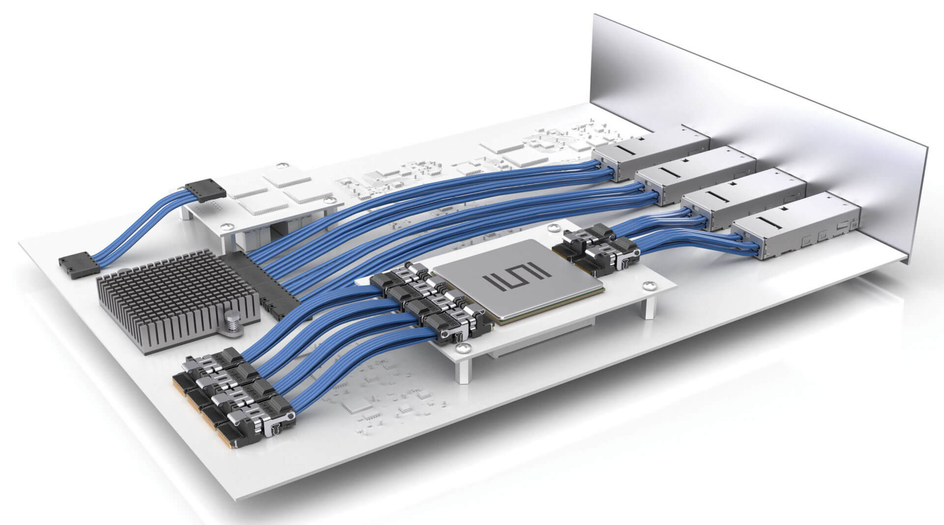
Martin then discusses one solution to alleviate the PCB loss problem, what Samtec calls “flyover.”
With flyover, high-speed signals are not routed through lossy PCBs, vias, and other components. Rather, they are routed through ultra low-skew twinax cable assemblies in system. This minimizes signal degradation while also eliminating the need for more expensive PCB materials.
Check out Martin’s article for a good explanation of the problem and a possible solution. And as luck would have it, I’ve included a few links to explain and elaborate on Samtec’s Micro Flyover System.™