The Samtec Microelectronics Group’s (SME) advanced packaging and high-speed interconnect expertise enable us to provide support for the performance, integration and miniaturization demands of next gen applications, including Connectivity, MedTech, MEMS & Sensors, and Optics, Imaging & Photonics.
Our advanced package design and glass core technology capabilities, along with standard design guidelines, are detailed in the new Microelectronics Interconnect Solutions Guide.
Microelectronics is part of Samtec’s Silicon-to-Silicon system optimization capabilities. Silicon-to-Silicon provides engineers the service, products, tools and resources to optimize the entire signal path, from bard die to IC package and assembly, to PCB, to connectors and cable assemblies, and back again.
The combination of packaging capabilities, proprietary glass core technology, and microelectronics system support equips SME to provide you with a unique level of support for advanced microelectronics applications.
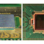
IC, MEMS, and Sensors Packaging Capabilities
Samtec Microelectronics provides complete design, assembly, and support for conventional and advanced packaging applications, including:
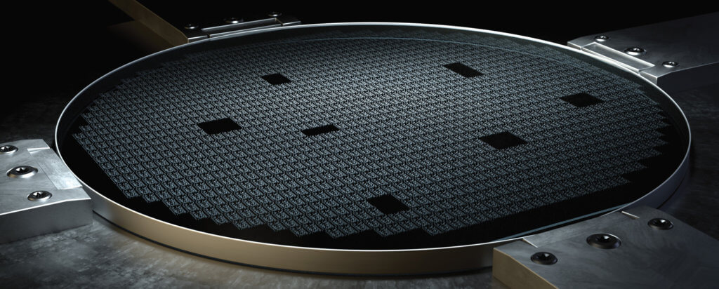
- Wafer dicing: Up to 8″ (203 mm) capabilities; thicknesses down to 25 μm
- Precision Die Placement: High-speed, high-accuracy die placement to +/- 3 microns
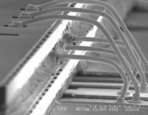
- Wire Bonding: Ultra-fine pitch, ultra-low profile ball bond, wedge bond, or ribbon bond
- Encapsulation: Encapsulating with dam and fill, glob top, or transfer molding (e.g., standard or optically-clear mold compounds)
- Advanced packaging solutions are enabled using the following capabilities:
- First-level interconnects
- Flip chip solder and gold stud bumps for tight pitches, down to 100 μm
- Fine-Pitch Flip Chip & Jet Underfill: Ultra-high bump count; low- and high-density bump regions
- Advanced substrates, inspection and metrology
- Glass substrate integration with various fan-out schemes
- Incorporating 2D, 2.5D, 3D TGV technologies
- Second-level interconnects
- BGA solder ball attach for tight pitches, down to 0.4 mm
- Package integration
- Package interconnects include electrical, optical, and fluidic types
- Lid attach – AuSn solder, glass frit, hermetic, and custom materials
- First-level interconnects
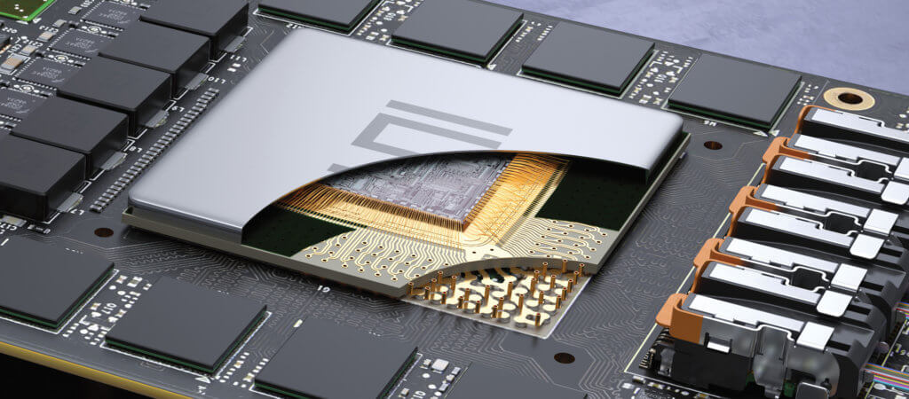
Glass Core Technology
Samtec’s propriety Glass Core Technology (GCT) process leverages the performance benefits of glass to enable performance optimized, ultra-miniaturized substrates for next generation designs. Glass substrates are well-suited for next generation microelectronics because they offer:
- High structural integrity
- Resistance to vibration, corrosion, chemicals, and temperature
- Environmental ruggedness
- Strong thermal isolation between temperature-sensitive chips
- Enhanced thermal performance (with dense TGVs and thermal ground planes)
- Low electrical loss
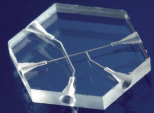
GCT substrate materials can range from borosilicate glass, fused silica/quartz, zirconia, and sapphire. GCT applications include automotive MEMS and sensors, smart building sensor modules, RF components and modules, advanced RF SIP, automotive RF, CMOS image sensor (CIS), automotive camera modules, active imaging and LiDAR, microfluidics and lab-on-chip, solid state medical imaging, and medical robotics sensors.
Microelectronics System Support
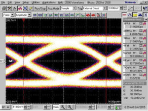
Samtec technical support and services are available at any level required. This focus runs from the early stages of the design process including package design, material selection and PCB routing, through in-depth analysis, modeling, and simulation, with measurement validation services available up to 67 GHz.
Teraspeed Consulting and Signal Integrity Group engineers help optimize and validate high-performance packaged products and systems. We can help with these challenges:
- Miniaturization and integration
- IC package, PCB routing, and breakout regions
- Complex or custom layouts
- Material selection
- Protocol compliance
- Cost control
- Power and thermal management