In this short video, Steve Groothuis, Chief Technology Officer for Samtec Microelectronics, explains Glass Core Technology (GCT), why it matters in advanced substrate packaging, and the solutions it provides.
GCT is a proprietary process that leverages the performance benefits of glass by creating small diameter, fine pitch Through-Glass Vias that are metalized and hermetically sealed.
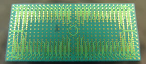
The TGVs are linked via a unique thin film Redistribution Layer (RDL) process to create custom circuits on a glass substrate.
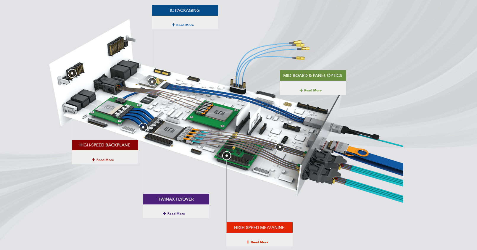
Glass Core Technology has at its basis the capability to provide engineering solutions for connectivity, biomedical, MEMS & Sensors, Optics & Photonics, and hermetic packaging platforms.
GCT uses borosilicate glass, fused silica, quartz, sapphire, and zirconia.
Glass Core Technology is a strong candidate for use in RF applications because of its excellent electrical insulation, low dielectric constant, high hermeticity, low warpage, and high resistance to corrosion.
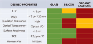
Compared to silicon and organic substrates, glass has superior performance, material characteristics, extreme miniaturization capabilities, and is rugged.
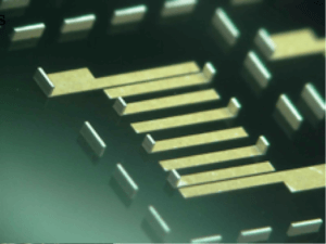
With today’s laser processing technology, GCT can address packaging solutions like high speed RF interposers, microstructured glass substrates for biomedical applications, and electro-optical package integration. The presence of laser technologies is found in glass micromachining, room temperature bonding of glass to silicon and glass-to-glass, and formation of microfluidic channels.
Glass has proven to be a key enabling technology for advanced packaging platforms.
- Glass interposers are beneficial for connectivity products that have RF, mmWave, Bluetooth Low Energy devices and used by telecommunication, defense, and Internet of Things companies.
- Microstructured glass substrates are beneficial as a platform for biomedical sensors, Lab-on-Chip, and microfluidic devices used by the healthcare and medical technology industry.
- Hermetic glass packages are extremely important for moisture- and particle-sensitive technologies like CMOS Image Sensors and are used by imaging, machine vision, and camera companies.
- MEMS platforms are used in 2.5D and heterogeneous integration, where different chip types are combined on a single substrate and are used by Internet of Things and sensor companies.
- Finally, Optical and photonics integration with electronic devices can truly benefit from incorporating glass elements within the light path of the resulting package.
Samtec’s Package Technology Roadmap reflects the evolution and revolution of Integrated Circuit, MEMS, Sensors, and Optical & Photonics packaging solutions going into the future.
For further information, please contact Samtec Microelectronics.