Centerlines to 0.4 mm. Gold plating that is 5μ” thick. Contact systems rated at 30 Gbps. Connectors that can handle 10,000 cycles.
While our expectations are high, we all know that developing the next generation interconnect solutions requires constant engineering and manufacturing innovation. And while connectors aren’t at the top of the electronics food chain, their role is critical in the successful functioning of any electronic system.
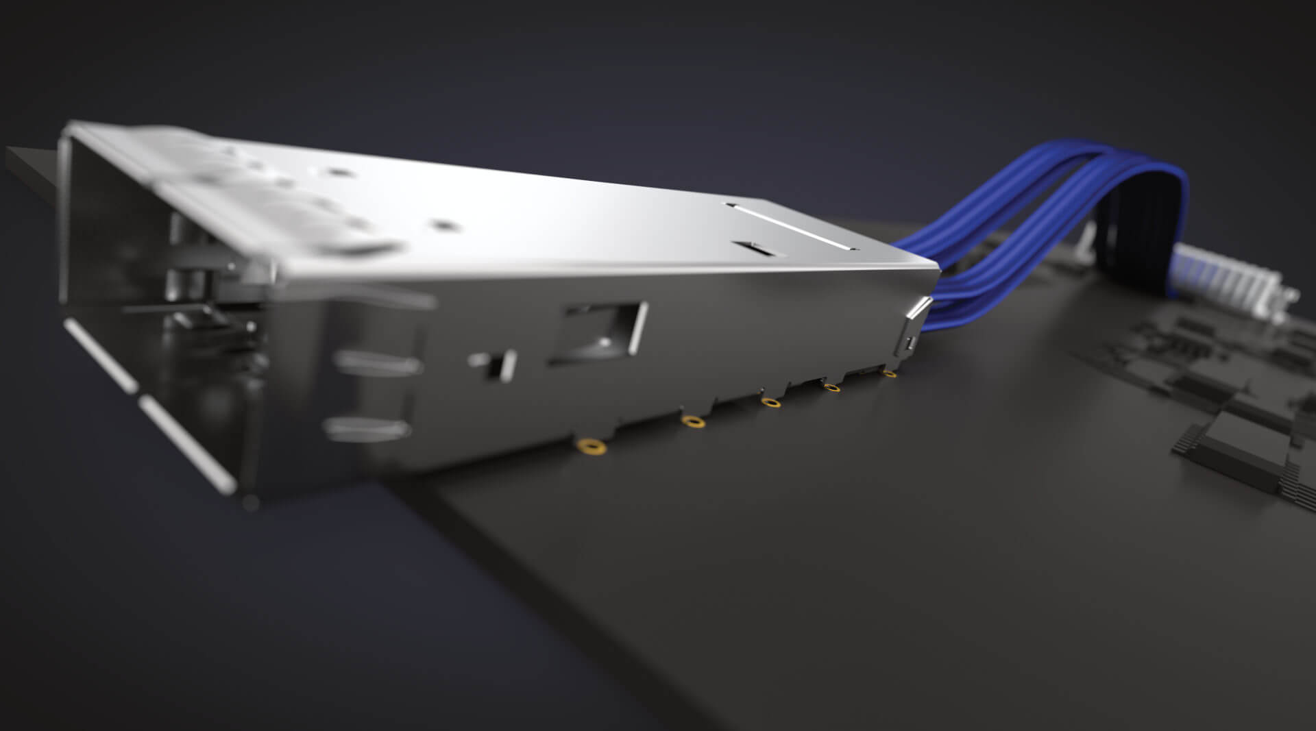
The Samtec Advanced Interconnect Design Technology Center (AID) ensures your interconnect systems are designed for quality, design flexibility, ease of processing, and even supply chain risk minimization. The AID includes precision stamping, plating, molding, and automated assembly for high-speed, fine pitch, array, and micro-rugged interconnects used for board-to-board, interposers, backplane, and high speed/high density cable assemblies.
Check out the new Advanced Interconnect Design Center video for a quick overview of the collaborative engineering and manufacturing techniques Samtec leverages in developing interconnect solutions that exceed customer expectations.
Samtec associate Dean Hohl summarizes the advantages of Samtec’s Technology Centers: “With our multiple tech centers, they all have areas of expertise or focal points, but the fact that we’re not divided … into business units allows us to work collaboratively, without these rigid boundaries that you find in most business units. And so innovation that happens in one tech center is easily transferred or shared with another tech center.”
Samtec Technology Centers:
- Microelectronics / IC Packaging: Precision die attach, ultra-fine pitch and low profile wire bond, flip chip, underfill, and dam and encapsulation, complete IC-to-board design, and support and manufacturing of IC packaging, substrates, micro high density interposers and micro optical engines. (video)
- Optical Group: Engineering team dedicated to the design, development, and application support of high performance micro optical engines, active optical assemblies, and high density ganged passive optical panel solutions. (video)
- Signal Integrity Group: In-house signal integrity expertise for complex applications, with live EE support available 24/7 worldwide. Advanced design support including Differential Vias™ and routing recommendations using Tri-Planar™ trace technology.
- Teraspeed® Consulting: Signal integrity services team providing complete system design, full channel signal and power integrity analysis and modeling, thermal management, and signal integrity-optimized advanced IC packaging for 28+ Gbps and beyond.
- High Speed Cable Plant: R&D and manufacturing of precision extruded micro coax and twinax cable used for high speed / high density cable assemblies, including 26-38 AWG, 50/75/85/100 ohm impedance, and systems rated at 28+ Gbps. (video)
- Advanced Interconnect Design: High precision stamping, plating, molding, and automated assembly for fine pitch and array interconnects used for board-to-board, interposers, backplane, and high speed/high density cable assemblies. (video)