Samtec Expert to Present at SEMICON West

Steve Groothuis, CTO of Samtec Microelectronics, in one of many panelists presenting at the Advanced Packaging Forum during SEMICON West next week at the Moscone Center in San Francisco, CA.
The Advanced Packaging Forum gathers executives, university researchers, engineers, R+D personnel, program managers and other technology experts across the IC packaging and assembly industry. Attendees you will learn about some of the latest assembly and packaging technologies—wafer-level packaging (WLP), fan out, and system in a package (SIP)—and how they will enable next-generation devices.

Mr. Groothuis will present on the topic “MEMS and Sensors Packaging – Leveraging More Than Moore Concepts” during the Advanced Packaging Forum session entitled “Sensing the Future: Enabling Applications for a Smarter World” on Thursday, July 14, 2016.
He will also provide insight into the design and assembly capabilities of Samtec Microelectronics. More information on the event can be found here.
Advanced Design and Assembly Capabilities
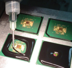
Samtec Microelectronics (SME) has an extensive, world-class offering of advanced package design and assembly capabilities as well as the ability to assist in choosing the best technology and materials for your specific application.
In addition to substrate and package design, flip chip, die attach, wirebond and sealing, our capabilities also include thermal management, wafer dicing, lid attach and marking. SME also offers support for multi-chip modules, interposer integration, ceramics, organics and glass substrates.
The following resources are designed to help release product to manufacturing as quickly as possible. For more information on Samtec Microelectronics design rules and guidelines, please download the following resources:
- Flip Chip Design Rules and Guidelines
- Die Attach Design Rules and Guidelines
- Wirebond Design Rules and Guidelines
- Dam Encapsulation Design Rules and Guidelines
Please send inquiries of pricing, support and technical detail to [email protected].