Samtec and Achronix Technologists Detail 112 Gbps PAM4 FPGA Implementation
Readers of the Samtec blog know we are always talking about next-gen speed. Current channels rates are running at 56 Gbps PAM4. However, system designers are starting to look at 112 Gbps PAM4 data rates.
Intuition would say that bleeding edge data rates like 112 Gbps PAM4 only occur in the data center. Why might that not be the case? FPGA vendors are releasing any number of new solutions featuring 112 Gbps PAM4 transceivers. FPGAs reside in a number of applications like 5G, AI/ML, Automotive and Test & Measurement.
How can system designers use the latest FPGAs for 112 Gbps PAM4 operation? How can signal channels be implemented from mid-board to front panel or mid-board to backplane?
Realizing 112 Gbps PAM4 Channels
Technical experts from Achronix and Samtec will answer these and related questions in an upcoming webinar: Accelerating to 112 Gbps PAM4 Webinar : A Real-World FPGA Implementation. What will attendees learn?
Accelerating data channels to 112 Gbps PAM4 forces system designers to balance increasing throughput, scalability and density demands with concerns such as signal integrity, system architectures and time-to-market. In this webinar, technical experts from Achronix and Samtec will discuss real-world tools and solutions that optimize the signal path both inside and outside the system design.
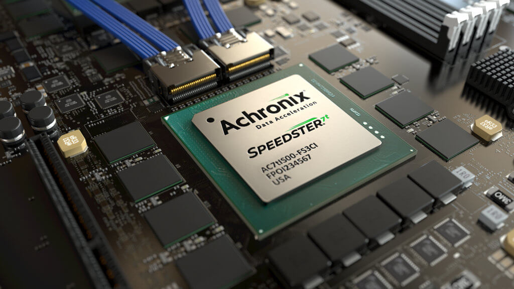
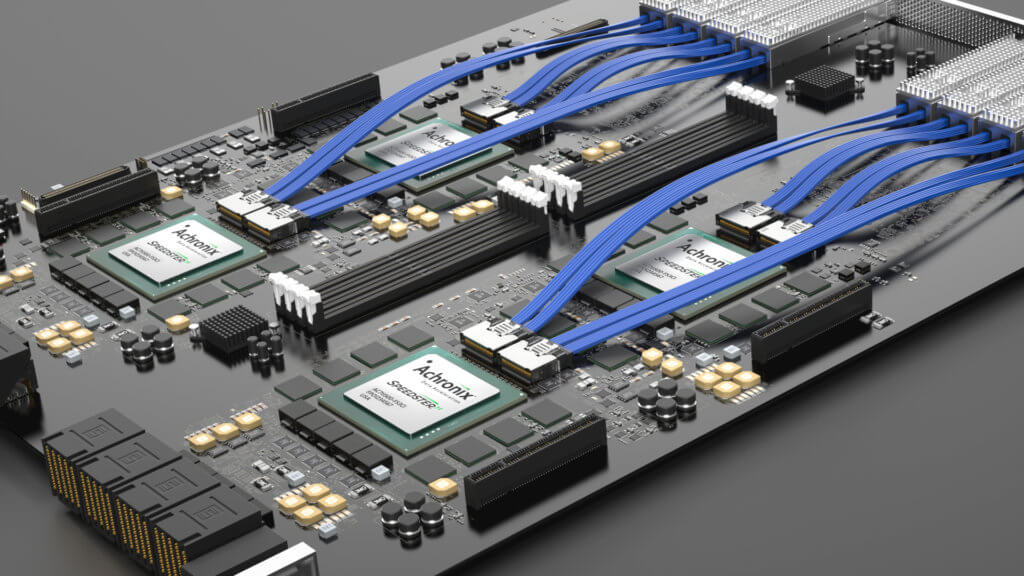
Achronix and Samtec will provide a real-world case study of implementing 112 Gbps PAM4 links using the Achronix Speedster®7t FPGA and Samtec’s portfolio of high performance interconnect solutions.
You will learn:
- What are some of the emerging applications that require 112 Gbps signals?
- How to optimize the FPGA SerDes settings for optimal signal integrity
- What are the key design considerations when designing your board interconnect?
Please register here to listen to the webinar on December 1, 2020 at 1:00 PM EST/10:00 AM PST.