
Designing and optimizing a breakout region (or component launch) for a connector can be challenging. It often requires multiple back and forth iterations and analysis to adjust variables. Samtec’s new SIBORGTM (Signal Integrity Breakout Region Guru) is a free tool that works with Ansys HFSS 3D Layout to generate, visualize, optimize, and develop PCB package and component breakout regions (BORs), enabling Samtec customers to design component launches faster. SIBORG was initially intended to be used during design collaboration with experts in Samtec’s Signal Integrity Group (SIG), but it can also be used independently by engineers to rapidly analyze different design variations that affect signal integrity in their connector BOR.
“It is imperative to understand electromagnetics and theory when optimizing vias and launches for high-speed PCB design,” says Scott McMorrow, Chief Technologist for Samtec and the developer of SIBORG. “An automated tool, such as SIBORG, allows designers to make small changes to layer counts, geometry, and transmission line characteristics, and see how that impacts performance without engaging in extensive calculations. And, by standardizing the variables used, SIBORG allows for more efficient collaboration between design teams.”
Variables that can be adjusted in the SIBORG tool include: dielectric variables, such as Dk; PCB manufacturing variables, such as the backdrill drill size; BGA pad geometry variables, such as center-to-center pitch between signal balls; via geometry variables, such as ground via pad diameter; antipad sizing variables, such as antipad in plane below trace layer; trace geometry variables, such as trace width; launch geometry variables, such as center-to-center pitch between signal vias; and BOR array generation variables, such as breakout direction vector. The Samtec SIBORG tool for Ansys HFSS currently supports 70+ variables in nine categories.
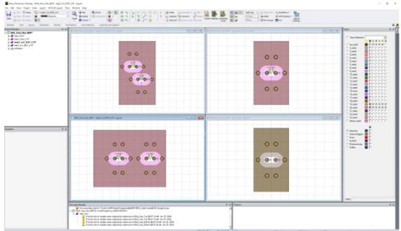
The SIBORG tool has easy-to-use drop-down menus to specify design parameters and generates images to allow engineers to quickly set up, visualize, and analyze the effects of changing the variables, allowing them to design component launches faster. The figure shows a screen shot from rendering a via-in-pad design. SIBORG tool can use all the capabilities of Ansys HFSS 3D Layout, including optimization and plot generation.
After the design is optimized in SIBORG, the results and s-parameters can be transferred to other tools for end-to-end channel simulation. Or, the designer can export the final design into a comprehensive module of PCB BORs and package/connector 3D models.
Introduced by Scott McMorrow during a tutorial session at DesignCon 2024, the Samtec SIBORG modeling tool for Ansys HFSS can be requested through the Samtec website. In addition, Samtec SI experts can be reached directly for design assistance or BOR optimization at [email protected].
Learn More
- Request access to SIBORG
- DesignCon 2024 Tutorial Slides on SIBORG
- McMorrow, Scott. Visualization of PCB Via Breakouts for Layout and Crosstalk Control, EDICON ONLINE April 24, 2024.
- SIJ Podcast on 224 Gbps and SIBORG
- Tips on Power Distribution and Breakout Region Design – The Samtec Blog
- Break Out Region Design By Inspection – The Samtec Blog


Leave a Reply