
Ok, I had a choice to make here with my opening statement; Ant-Man (which is more timely and goes to the quantum level) or go old school with “Honey I Shrunk the Kids.” Clearly the choice here was Rick Moranis combing his back yard with a magnifying glass to find his shrunken kids.
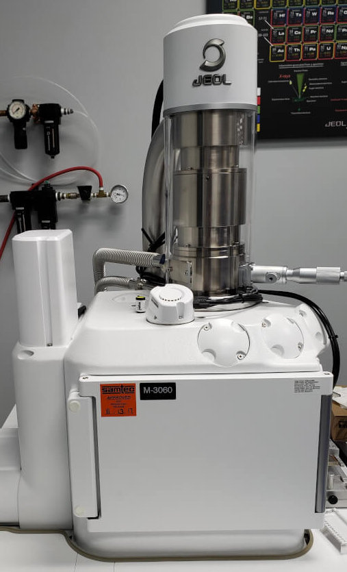
While a magnifying glass is not a Scanning Electron Microscope (SEM), Rick was scanning his yard with a magnified view much like engineers often have to rely on technology to help us solve problems on a tiny scale. In the connector world, we have started utilizing high-speed cameras to analyze production machines, and in the test lab, Scanning Electron Microscopy is being utilized.
What is a Scanning Electron Microscope (SEM)?
A scanning electron microscope (SEM) is an analytical tool that is used for visual imaging and chemical composition detection. The SEM operates by sending a focused beam of electrons that interact with the surface of the sample item.
The electron beam is sent into a vacuum chamber where the sample is held. The electrons then interact with the sample creating secondary electrons, backscattered electrons, x-rays (photons), and several other signals.
The electron signal can provide an engineer with needed information about the sample including: chemical composition, surface measurements, external morphology, and even crystalline structure of the sample.
A typical SEM can have a magnification range of 20X up to 30,000X with some even going to 1,000,000X. The spacial resolution of a SEM is around 50 to 100 nm, and is capable of of analyzing pin point locations.
How does Samtec use the SEM?
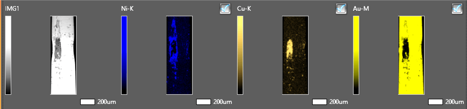
Samtec utilizes the SEM to identify / inspect wear patterns (as shown above), identify chemical makeup of surface substances, measure plating thicknesses, and identification of tin slivers and whiskers.
The image above shows a colorized elemental map of the surface of a pin after cycling. Samtec utilizes these images/information to determine the cause of failure during a test, or to determine if a connector can be used for further testing. This is useful in that as the gold is removed, the resistance is likely to increase.
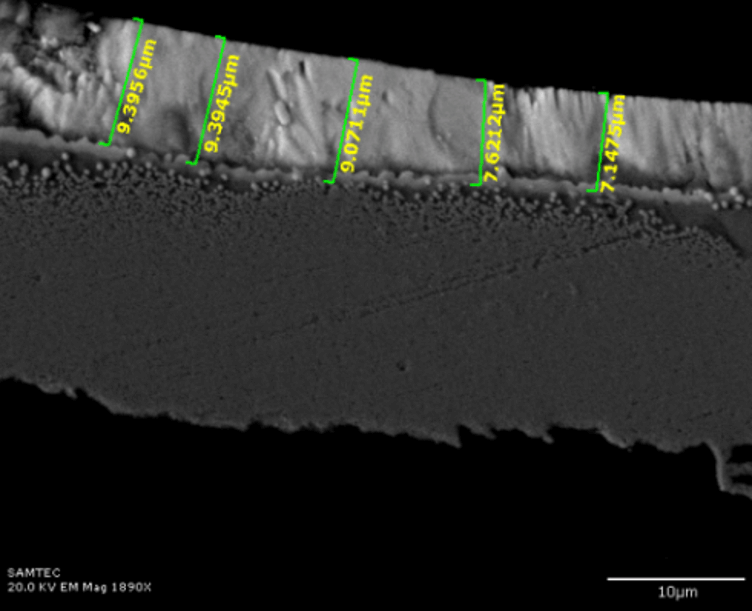
The SEM is also useful in measuring plating thickness, by layer, after the part has been cross-sectioned. This can help determine what areas of the pin could be prone to failure, and how to adjust the plating process to ensure proper thickness according to location.
Using the SEM is just one part of what Samtec does for part qualification and failure analysis. Make sure to check out the other blogs on our testing capabilities:
- Understanding Low Level Contact Resistance (LLCR)
- Insulation Resistance and Dielectric Withstanding Voltage Testing
- Thermal Shock Testing for Connectors
- Testing the Effects of Humidity on Connectors
- Using Nanosecond Event Detection to Identify Effects of Mechanical Shock and Random Vibration
- Mechanical Shock and Vibration and Your System
- Severe Environment Testing


Leave a Reply