Samtec’s gEEk® spEEk webinars allow engineers the opportunity to interact with Samtec’s engineering leaders and SI experts on a variety of selected SI-related topics.
Gustavo Blando, a Samtec Signal Integrity Architect, recently presented “DC Block Capacitor Location (Does It Matter)?” I spoke to Gustavo about his presentation and why he selected the topic, and the challenges in selecting the location of DC block capacitors. As you can probably imagine, it’s more complicated than you might think.
DANNY: Gus, why did you select this topic for a gEEk spEEk webinar?
GUSTAVO: My high school physics teacher once told me, “If by 22 years old you haven’t discovered anything, I can guarantee you will not be a genius, but don’t despair since you can still be very experienced.” I’m in my 40s and I have not achieved either!.
This became evident when I was thinking about the never-ending argument of where to place a DC blocking capacitor in a high speed serial link.
There are two compelling arguments: The first argument is, put the DC blocking capacitor close to the receiver and you’ll be good, since all of the reflections will be smaller due to transmission line attenuation. This represents a time domain view of the world.
The second argument is, for most passive interconnects, S-parameters are reciprocal (S21 = S12). Under this pretense, for a particular topology, as long as the distance from the end points to the DC blocking capacitor is the same, it does not matter if you place the capacitor at the receiver or driver, because the results will be identical. This represents a frequency domain view of the world.
DANNY: I’m not going to comment on your Physics teacher’s comment because it hits too close to home. But, can you elaborate on those two topology theories?
GUSTAVO: If you start peeling away at the layers of this paradox, you quickly realize that this is a tricky question, and it all boils down to how you ask it. Let me explain with an example.
Let’s say we have two topologies. Both include a driver and a receiver with the same output/input impedance, a couple of transmission lines of different lengths, and a symmetrical (S11=S22) connector somewhere in the middle.
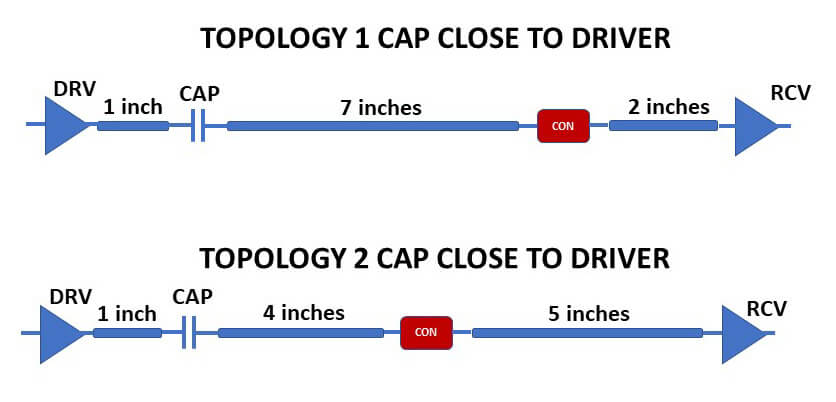
Let’s look at Topology #1 first. If we agree with the second argument, we should conclude that changing the location of the capacitor and placing it 1 inch from the receiver as shown below, should provide the same voltage at the receiver, right?
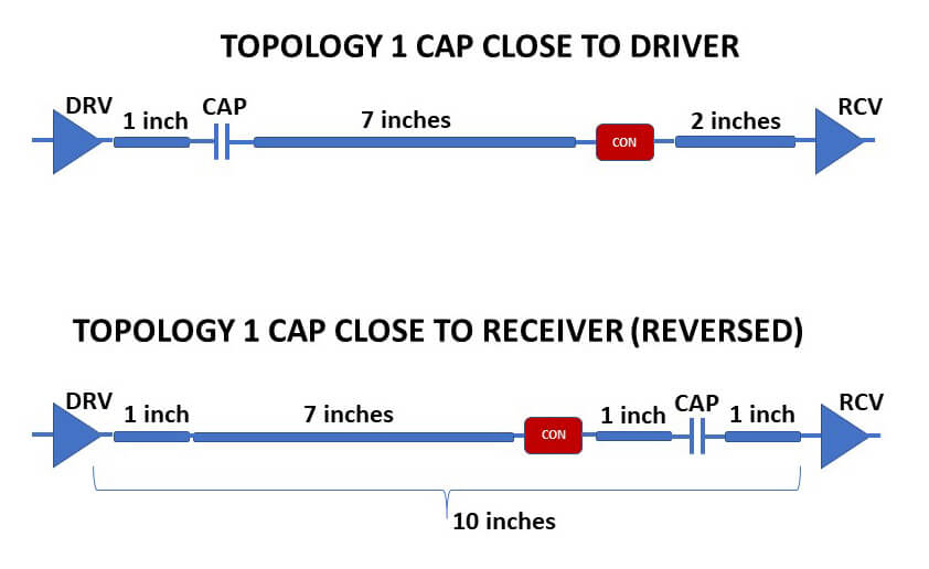
Trust me for now, but this is wrong!
Now, let’s look at Topology 2, and let’s do the same analysis.
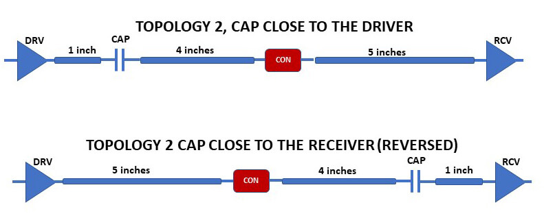
If you trusted me before, you would conclude the voltage received at the RCV in Topology 2 and in Topology 2 Reversed would also be different, correct?
But, this will also be wrong! In this case, the results for Topology 2 and Topology 2 Reversed will be the same, meaning the voltage at RCV will be identical.
DANNY: Uh, OK. Help me out here. Why are Topology 1 and Topology 1 Reversed different?
GUSTAVO: In order for those two topologies to produce the same results at the receiver, S21_Top1 should be the same as to S21_Top1R. The spatial relationship between the connector and the DC blocking capacitor changes depending on which side of the connector the DC blocking capacitor is placed. This will result in a different insertion loss (S21) between these topologies and hence the results will not be the same.
DANNY: I’m almost afraid to ask, by why are Topology 2 and Topology 2 Reversed the same?
GUSTAVO: Take a careful look at Topology 2. Then look at it again, but look at it from left to right, and compare that to Topology 2 Reversed. You probably noticed that Topology 2 Reversed is exactly the same as Topology 2 from the left? Or in other words, swapping the DRV and the RCV on Topology 2 will result in Topology 2 Reversed.
This means S21_Top2 is exactly the same as S21_Top2R, since we know the S-parameters are reciprocal. In this case, placing the DC blocking capacitor at the driver side or at the receiver side would be exactly the same.
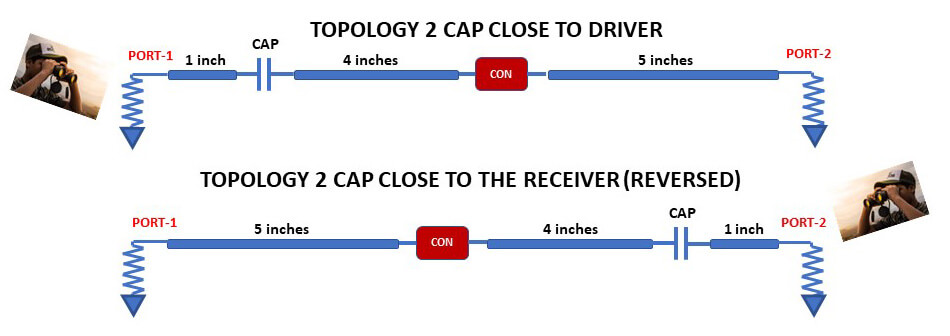
Also, in the initial formulation of the question I mentioned the connector is symmetrical (S11=S22). I will leave it to you to decide what would happen if this was not the case 😊
DANNY: OK, but you never told me where is the best place to put my DC blocking capacitor? What is the best location?.
GUSTAVO: As every well-respected signal integrity engineer will tell you, my answer is “it depends.” If you want to dig a little deeper, please feel free to go to the gEEk spEEk presentation where I elaborate on this question.
But regarding your question, let me just conclude by saying loss is your friend.
DANNY: You may also be interested in these other gEEk spEEk-related interviews: PCI Express: Is 85 Ohms Really Needed? and Channel Operating Margin: An In-Context Channel Compliance Method.


Hi Danny,
This is very simplified capacitors placement analysis in the serial link system where the decisions were based on the transmitter, receiver and connector impedance equal or closely to the trace impedance. If the system has a different impedance on each part, the different reflections coefficients, trace lengths and as result reflected signals propagations will produce the different jitter and voltage noise on the receiver 🙁
Regards,
AlexS