Practical Guidelines To Achieve Quality Connector Solder Joints: Part One
Many factors affect the quality and performance of a connector: pin material, the quality of the stamping, the quality of and choice of surface finish, and the tolerances on the plastic insulator, just to name a few. Beyond the connector, another factor that is crucial to the performance of the connector on the printed circuit board is the quality of the solder joints.
This is the first in a series of three blogs, which are interviews with David Decker, the Manager of Samtec Interconnect Processing Group (IPG). In these blogs, David answers some of the most frequently asked questions about connector solder joints.
The goal in answering these questions is to provide a short answer that addresses the main issue; we don’t want to present a “mini whitepaper” for each question. Of course, please contact the IPG if you have questions, need more information, etc.
BTW, here’s the link to the second blog in this series, and here’s a link to part three.
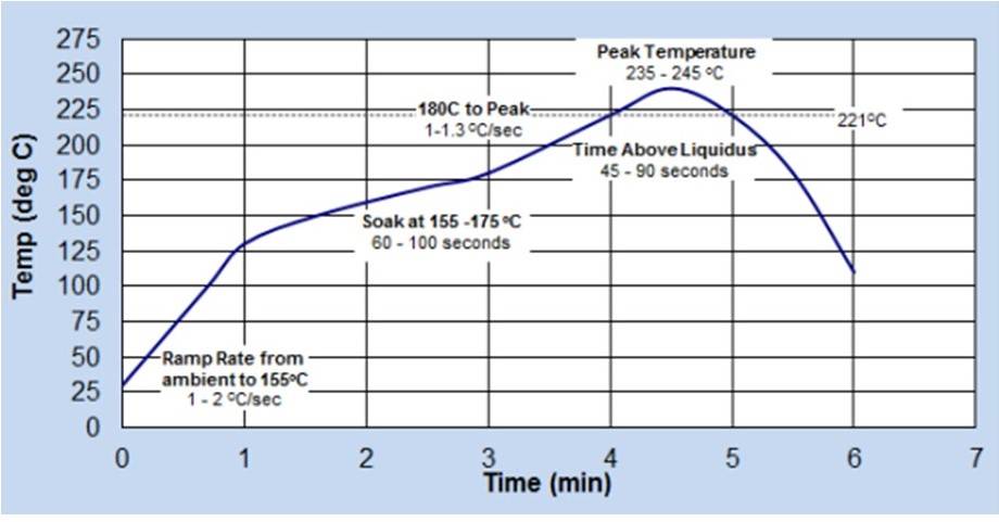
At what peak temperature are most SMT ovens run?
DD: This is probably the most commonly asked question we receive in IPG. The answer is always the same: the peak temperature is the derivative of the solder paste that you use. Our SMT and SMT-compatible through-hole connectors can handle 260° C with no problems. Having said that, most of our customers run their ovens at significantly lower temperatures, usually between 235° and 245° C, for a lead-free profile.
The reason most of them moderate their temperature is to make sure they are not damaging other heat-sensitive components. So when we are asked that question – what is the peak temperature for SMT oven processing — our answer is to consult the solder paste manufacturer and see what they recommend for their specific paste.
Will my solder paste work with Samtec connectors?
DD: The answer is probably yes. Our connectors are widely used, and there are many solder paste manufacturers. We use Alpha solder pastes, which are ubiquitous. Specifically, Samtec uses the following Alpha solder pastes:
- SAC (lead-free)
- WS-820 (Water Soluble)
- OM-338 PT (No Clean)
- Tin-Lead
- WS-809 (Water Soluble)
- OM-5100 (No Clean)
We have many customers using many different pastes, and we try to make all of our connector devices as robust as possible, so that the connector is not the gating item in your processing endeavors. So again, the answer is yes, your solder paste will work with Samtec connectors, with very few exceptions.
Are there any new soldering materials that are gaining interest?
DD: We see a lot of interest in low-temperature solder paste. Of course, lead-free technology requires higher temperature processing. The melting point of most SAC lead-free solder pastes is about 217° C, and that’s up from approximately 183° C for tin-lead solder paste. That’s a significant jump in paste melting temperature. With that delta, from tin-lead temperatures to lead-free, many customers are concerned about component warpage, and potential discoloration of heat-sensitive devices and platings.
Solder paste manufacturers are working on other chemistries and technologies to lower the processing temperature. The ones we see the most with regard to lowering that melting temperature contain bismuth or indium. These new pastes can lower the melting temperature to 140° C. And we know that every benefit has a disadvantage, and the primary disadvantage with these low-temperature pastes is brittle, less robust solder joints.
In my opinion, there’s still some work to be done by these solder paste manufacturers.
Should I pre-bake my components prior to soldering?
DD: Samtec connectors, and SMT connectors in particular, do not require pre-baking. Per IPC/JEDEC J-STD-020E, our connectors do not require pre-baking because the moisture sensitivity level of our connectors is 1. Some customers do decide to pre-bake, and it’s not going to hurt the connectors. The need for pre-baking is because of entrapped water in the device or component; pre-baking evaporates any trapped water content in that device/component.
Pre-baking might be more of a concern if your inventory or manufacturing facility is located in a place with higher humidity levels.
If a connector coplanarity spec is .006”, what stencil thickness should I use for the best solder joints?
DD: This is another question that we are asked just about every day. A connector coplanarity specification of .006” (0.15 mm) is common for bigger connectors (for example, on .100″ pitch, with 15 or more pins). It makes sense to think that the stencil has to be as thick as the coplanarity spec. At the same time, other devices on the same board may require a thinner stencil, for example, .004” (0.10 mm). It’s possible that using a thicker stencil could lead to other problems, like solder joints bridging.
At Samtec, IPG works with the connector designers in the new product development process. When we begin testing the soldering process, we use a .004”, .005” and .006” thick stencil, and we use varying aperture designs, to optimize the stencil design. So our stencil recommendation has been fully vetted, and we know what works and what doesn’t work, for the most part. Unless it fails in our testing, a .004” stencil can be used. And likewise, rarely does a .006” stencil not work. We have stencil thickness recommendations on the product pages of our website (here’s an example). All of the details of these recommendations have been tested and can be trusted.
We recently completed a solder joint study with Phoenix Contact about using solder stencils on connectors that are thinner than the connector’s coplanarity spec. This study shows you can successfully solder connectors with a .006” (.15 mm) coplanarity spec using a .004” (.10 mm) thick stencil. A customer might have to do this because they have other devices that require a .004” thick stencil, or because they don’t have the time or budget to handle the expense of using a stepped stencil.
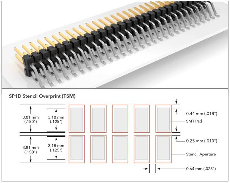
In this study, we designed the stencil apertures to be bigger than the pads on the PCB (i.e., overprinting). The solder that’s printed beyond the pad in all four directions will coalesce and flow back onto the pad and lead during the reflow process. We didn’t experience solderballing or other problems.
More on Solder Joints and Soldering …
If you want to learn more, stay tuned. We will post at least two more blogs in this series. If you have any questions in the meantime, please contact the Interconnect Processing Group.
IPG has tons of experience helping customers solve their processing and design challenges. We understand that every design is different and has its own unique issues. IPG can assist you in improving the overall processing and manufacturability of your board as well as helping lower its total applied cost.