Practical Guidelines To Achieve Quality Connector Solder Joints: Part Two
This is the second in a series of three blog interviews with David Decker, the Manager of Samtec’s Interconnect Processing Group (IPG). In these blogs, David answers some of the most frequently asked questions about achieving quality connector solder joints, as well as other connector-processing-related issues. BTW, here’s the link to the first blog, and here’s a link to the third one.
Our goal is to provide short answers that address the main issue of the question. If you want more information about a particular subject please contact Samtec’s Interconnect Processing Group.
What are common problems with two reflow oven passes and inverted components?
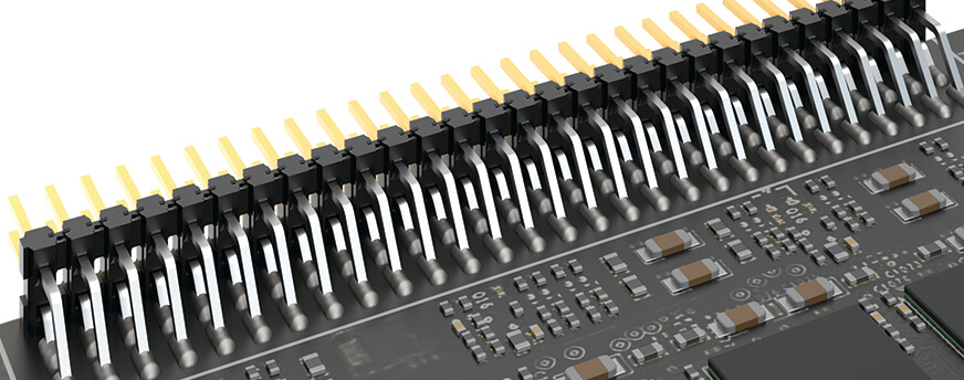
This is a common question because this is a common processing method. Our connectors are typically some of the smaller components on a PCB and therefore are typically lightweight. Usually, PCB-level components are on side one of the PCB; the paste gets printed, the components are placed, and the board is run through the oven.
After this pass, the board is inverted – meaning our connectors are now upside down. The larger devices and the heat-sensitive components are usually placed on side two, and the board goes through the oven the second time. So, our connectors go through two oven passes, and they are inverted on the second pass. Most customers are able to process almost all Samtec connectors in this manner, with no problems.
As part of our product qualification testing, we send our connectors through the oven three times: once on a standard soldering pass, and then twice on inverted passes. Almost all of our connectors pass these tests because almost all of our products are small and symmetrical, so the surface tension of the molten solder will hold the connector to the PCB while it’s inverted, without the need for additional hold-downs, locking features, or glue. Connectors that are more challenging are generally larger with an offset center of gravity.
Are the common board processing problems experienced in recent years different from those of 10-20 years ago?
The short answer is yes, primarily due to miniaturization. Components are getting smaller, stencils are getting thinner, and designers are trying to squeeze more parts on smaller boards. All of this adds up to processing challenges.
But, stencil design technology continues to improve, solder pastes are getting better, and reflow ovens are more precise and reliable. In other words, the tools used to create and inspect solder joints seem to be keeping pace with the demand for miniaturization.
What do the different IPC solder joint classes mean?
IPC, the Institute for Interconnecting and Packaging Electronic Circuits, is the recognized governing body for the inspection of solder joints in electronic assemblies. IPC separates solder joints into three classes.
Class 1 is for “General Electronic Products,” meaning if these products fail, it’s a nuisance to the user or they experience an inconvenience. Children’s games and toys are an example of products with Class 1 solder joints.
Class 2, or “Dedicated Service Electronic Products,” is a significant step up in terms of functionality and reliability. If this product fails, the user’s inconvenience and “annoyance factor” is much greater than Class 1, but the user does not face physical harm. Samtec connectors are IPC Class 2.
Class 3, or “High Performance/Harsh Environment Electronic Products,” refers to high-reliability products where performance is critical. Examples include military, aerospace, and medical applications. If these solder joints fail a person might be injured or even killed. A significant number of Samtec connectors are rated IPC Class 3.
An IPC Class 3 rating doesn’t mean every time an EOEM solders a connector they achieve a Class 3 solder joint. Other factors come into play, such as stencil thickness, the precision of the connector placement, and pad design, to name a few.
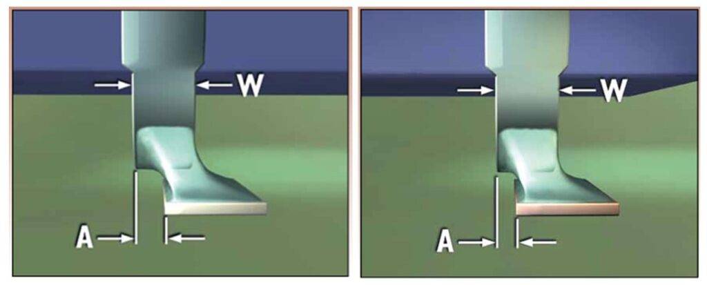
The illustration above shows the difference between a Class 2 vs. Class 3 solder joint. Dimension W is the width of the component lead, and dimension A is how much of the lead is extending over the solder joint/PCB pad. For Class 2 solder joints, A can be one-half of W. In other words, 50% of the lead can be “off” of the side of the pad. For a Class 3 joint, A can only be 25% of the width of W. This is just one quick example that illustrates the differences between Class 2 and Class 3 solder joints. Here’s a link to learn more about the differences between Class 2 vs. Class 3 solder joints.
Do I need to do anything special if I am conformally coating my PCBA?
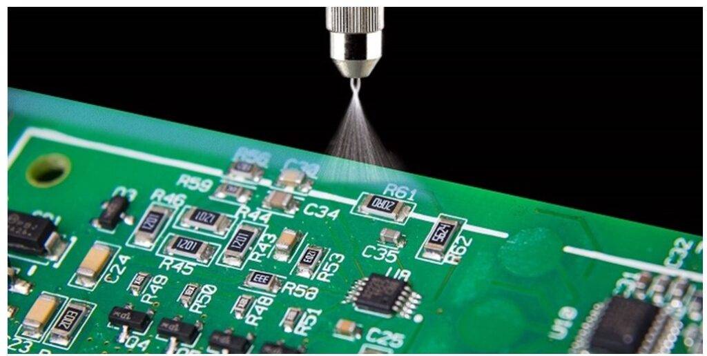
Conformal coating is a common practice. One of the biggest challenges in preparing a PCB for conformal coating is to protect the contact surfaces, which are typically internal to a socket strip connector, but not always. Also of concern are exposed terminal strip pins for an unshrouded connector.
Masking becomes important in these applications. Here’s a link to a document that discusses several of the more commonly used methods of applying conformal coating as well as masking methods.
Parylene conformal coating is popular. This is a complex process that requires significant masking. The Parylene process involves taking the PCB assembly and placing it into a chamber where a vacuum is pulled. As the vacuum is pulled, the Parylene coating is introduced into the chamber and it goes everywhere air can go, allowing the Parylene to get into every nook and cranny of the connector(s). As you can imagine, it’s very difficult to mask all of the critical areas. If a customer asks us about the Parylene process, we refer them back to the Parylene manufacturer.
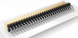
If there is a solder joint problem with an array connector, how do I rework it?
As the name implies, array connectors are larger and they typically have an X, Y grid of positions. Samtec grid array connectors frequently have 500 or more I/Os on a single connector. If an internal solder joint on an array connector has a problem – and the vast majority of solder joints on an array connector are internal/under the insulator – your only recourse is to remove that connector and replace it with a new one.
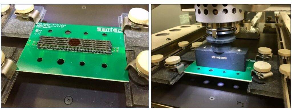
Simply described, the process involves placing the PCB into a hot air rework station. A nozzle is placed on the top of the PCB, just above the surface, but surrounding the connector. A prescribed thermal profile is executed where hot air is introduced around the array connector, the solder melts, the nozzle is lifted off the PCB, and the connector is literally removed from the board using pliers or tweezers.
The board will need to be cleaned and the old solder removed. Our Air-Vac rework system blows hot air on the solder to keep it molten, and a nozzle removes the solder. Once the solder is removed, the rest of the PCB is cleaned. Then, using a mini-stencil, fresh solder paste is printed on that PCB. A new connector is placed on the PCB, the hot air nozzle is placed over the connector, and a profile is run to resolder the new connector. Although it sounds complex, this process works very well.
Samtec recommends maintaining an approximately 1/8” (3.175 mm) “keep out area” around the connector to leave room for this rework system, on the slim chance it’s needed. Here’s a link to learn more about this process.
More on Solder Joints and Soldering …
If you want to learn more, stay tuned. We will post the third blog in this series soon. If you have any questions in the meantime, please contact the Interconnect Processing Group.
IPG has tons of experience helping customers solve their processing and design challenges. We understand that every design is different and has its own unique issues. IPG can assist you in improving the overall processing and manufacturability of your board as well as helping lower its total applied cost.