Practical Guidelines To Achieve Quality Connector Solder Joints: Part Three
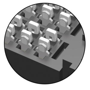
Beyond the construction of the connector, another factor that is crucial to the performance of the connector on the printed circuit board is the quality of the connector solder joints.
This is the third in a series of three blogs, which are interviews with David Decker, the Manager of Samtec Interconnect Processing Group (IPG). In these blogs, David answers some of the most frequently asked questions about connector solder joints.
As stated previously, the goal in answering these questions is to provide a short answer that addresses the main issue; we don’t want to present a “mini whitepaper” for each question. Of course, please contact Samtec’s Interconnect Processing Group if you need more information, etc.
Previous Blogs About Achieving Quality Connector Solder Joints
- Practical Guidelines To Achieve Quality Connector Solder Joints – Part One
- Practical Guidelines To Achieve Quality Connector Solder Joints – Part Two
What is the benefit of using an inert gas reflow oven environment? Does this improve the strength of the connector solder joints?
The term “inert” usually refers to nitrogen gas, which can be infused into a reflow environment to displace oxygen. This minimizes the opportunity for oxidation because oxygen promotes oxidation. The oxygen corrodes and forms a “skin” over the solderable surfaces and the solder itself, which inhibits wetting.
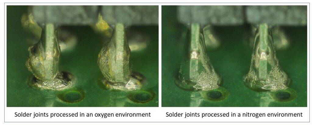
The pictures above show connector leads from an array connector that were reflowed in an oxygen environment (left) and a nitrogen environment (right). The solder joints on the right wet better and are more uniform, and they are simply brighter. All of this is because oxygen was not present.
If you have the opportunity, and if the economics allow, we encourage the use of nitrogen in the reflow process. Samtec tests all of our new products in both oxygen and nitrogen environments.
What are the pros and cons of using paste-in-hole (PIH) technology?
Paste-in-hole (PIH) technology has been around for years, and it’s becoming more popular as the miniaturization of PCBs proliferates. If the majority of the components on the PCB are SMT, with the balance being through-hole (TH), it’s possible to process the TH components at the same time as the SMT components.
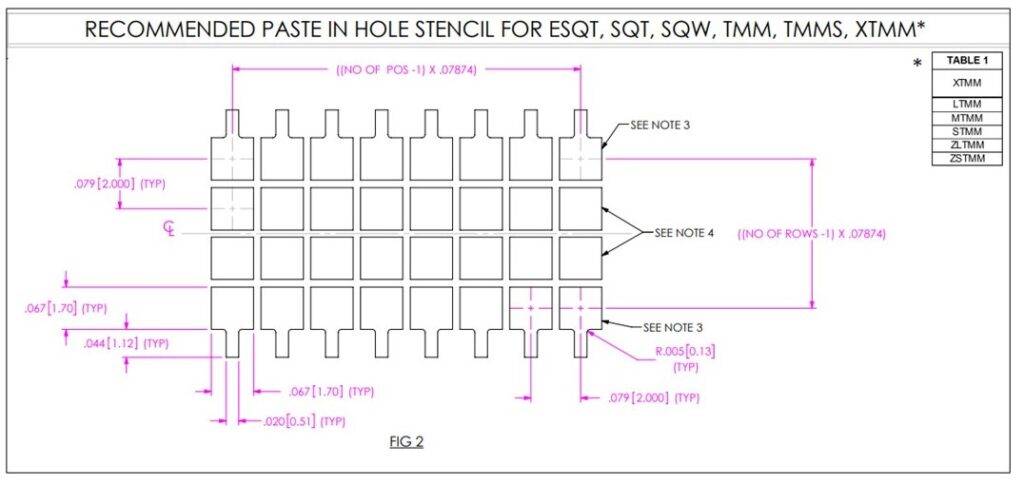
This is accomplished by printing solder paste over the entire PCB, including the plated through holes (PTH) which are used with the TH components. Some of that solder paste will go into the PTH, and some will go around the PTH. Notice the large, square apertures in the recommended stencil design above. The TH components are placed in the same manner as the SMT components; this is possible because of the precision of today’s pick-and-place equipment.
With PIH, all components are placed on the PCB and sent through the reflow oven. The solder paste that is in and around the PTH flows into it, forming a strong solder joint. This reduces your processing steps from two to one.
Designers must make sure the materials in the TH connector can withstand the elevated temperatures of the reflow process and that there is room to print the solder paste on the PCB so that the connector doesn’t sit in the wet solder paste. The latter is typically accomplished through plastic standoffs on the connector. Of course, of most interest is the type of plastic used in the connector body or insulator. Here’s a blog with more information about Paste-In-Hole Reflow Processing.
Do connectors self-center during the reflow process?
Don’t I wish! That would solve a lot of problems, especially in applications with multiple connectors on the PCB. But the answer is, in general, no. Flat gull-wing or J-style leads simply don’t have the self-centering capabilities of solder ball products.
Solder wants to reside in the most stress-free geometry, which is a sphere. Solder is most at rest, or stress-free if it is spherical (or ball) shaped. When the entire connector is resting on a solder sphere or ball, and on solder paste that contributes to the size of that ball after it reflows, it does a much better job of self-centering. The video above demonstrates this. The connector with the solder ball leads is intentionally offset about half the pad width, and as the solder reflows, it pulls the connector over the center of the pad. Please note this is a short video; we suggest watching it several times.
What is solder charge technology?
We always want to get more solder in the solder joint. This can be accomplished by printing more paste on the PCB, or you can attach solder to the lead (i.e., a solder-bearing lead), and that’s what solder charge technology is. It’s a clag of pure solder, no flux, that is mechanically attached to the tail lead of the connector. For example, our SEARAY™ product line uses solder charge technology. Solder charges allow you to place more solder in the joint area to form a more robust solder joint.
A loop in the connector contact tail helps hold the solder charge to the lead. The video above illustrates this process.
As mentioned above, the only flux with solder charge technology is what’s in the solder paste. Therefore, it is critical that customers follow our stencil recommendation guidelines, that the connector is properly placed on the PCB, and that sufficient solder paste is placed on the PCB.
If you have any questions please contact the Interconnect Processing Group. IPG has tons of experience helping customers solve their processing and design challenges. We understand that every design is different and has its own unique issues. IPG can assist you in improving the overall processing and manufacturability of your board as well as helping lower its total applied cost.