Selecting a backplane design requires tradeoffs specific to a particular network topology and application. In some cases, the assessment of PCB vs cable backplane is not an “either/or” but a combination approach. This blog post, based on a conversation with Samtec’s Andrew Josephson, Brandon Gore, and Jonathan Sprigler, aims to answer some of the most common questions that come up when deciding should I use a PCB or cable backplane for a high-speed design?
How do the two approaches compare on cost?
Like most engineering answers…it depends. It depends on the physical reach of the fabric segments, the number of lanes each segment must carry, the number of physical net crossings the network creates, the need for the serial fabric to co-exist with other system infrastructure, and the scope of the backplane design itself. For physically simple serial fabric topologies with limited-scope design efforts, the cost tradeoffs can be simple to evaluate. But for complicated topologies and large-scale system development efforts where development schedule, early hardware/firmware/software intersection enablement, and total cost of ownership become value criteria, the answers to how the approaches compare on cost can become more complex.
At the BOM level, a cable backplane can be more expensive than a traditional PCB one. But, at the system level, cable backplanes can offer significant advantages by enabling earlier software development/integration activities and lower total cost of ownership on the back end. For instance, a cabled backplane can interface blades with test equipment, software development platforms, and early engineering proto-systems, all while offering high enough performance to future-proof the production solution.
Samtec offers traditional right-angle board-to-board backplane connectors with cabled options for exactly this reason. Some applications value these solutions purely for SI performance, some value them for flexibility in development and integration, some value them for both. And finally, some developments are well suited for buy-versus-make decisions. Procuring COTs cable assemblies from a component supplier can sometimes simply be faster/easier/cheaper than designing a custom high-performance backplane PCB programmatically.
Which backplane is better for different network topologies?
Figure 1 shows the physical mappings for some common network topologies. In more complicated network topologies with many more segment crossings, cabled backplane approaches can run into scaling issues, making PCB route approaches more attractive. Additionally, PCB-based backplanes can offer advantages for co-design with other infrastructure, such as power delivery and out-of-band low-speed signals.
In the case of the simple ring, mesh, and star topologies, using a cable backplane might allow the nodes to be populated at an increased blade or module pitch (accommodating thermal design space as component power densities increase, or potentially placed in adjacent racks or chassis).
Look at the star topology that is outlined in the rack/chassis depicted in Figure 1 (right). In this example, the node or blade has the same design with the same connectors for either a cable or PCB backplane. This means designers can plan for a PCB backplane now with the ability to migrate to a higher-speed cable backplane later, or design for a cable backplane today to achieve extra margin.
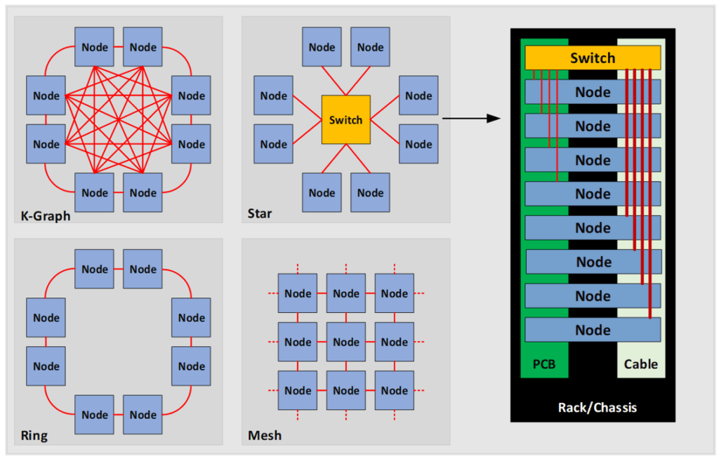
Figure 1: (left) Different network topologies have different physical mappings. The “star” configuration is perhaps the most common. The star topology is also depicted in a rack (right), showing where one might use PCB and cable backplanes in a combined configuration.
How does performance compare?
Both PCB and cable backplanes can offer excellent performance at shorter channel links. Cable backplanes can also provide excellent signal speeds at longer channel links. One reason cable backplanes can do this is that the traces are not running through the PCB, so each of the differential pairs can go through an individual shielded cable. This can lead to less loss and better signal integrity vs a PCB channel (see Figure 2).
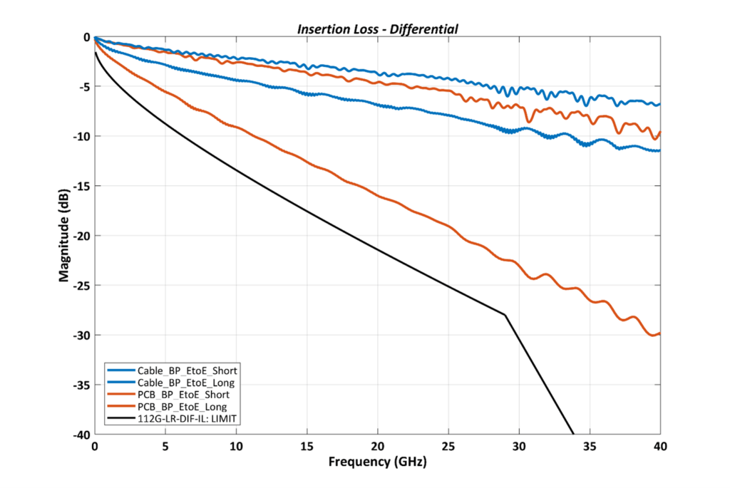
Figure 2: A comparison of insertion loss for 4-in and 18-in cables (blue traces) and 2-in to 16-in PCB backplanes (orange traces). The black line shows the industry standard insertion loss limit.
In Figure 2, all the options work within the design parameters out past 35 GHz, and they offer a 5- or 6-dB design margin, which traditionally has been enough to accommodate loss issues in the system design. But is that enough for next-generation systems? Answering this requires performing system level channel analysis (see next question).
How much performance is needed for 112 Gbps PAM4?
Higher data limits, such as CEI-112G-LR-PAM4 [3], and IEEE 802.3 400GBASE-KR4 [4] lead to loss of margin at the system level, especially when designing systems for cost effectiveness. When eight lanes are plotted and system level losses against PAM4 requirements are assessed using channel operating margin (COM), for instance, a 5 or 6dB margin starts to get strained (see Figure 3).
In this model of 800 GbE ports, each lane acts as a victim while the seven other lanes act as near-end transmitting aggressors. In Figure 3, the green points are at CEI-112G-LR-PAM4 while the orange are at IEEE 802.3 400GBASE-KR4.
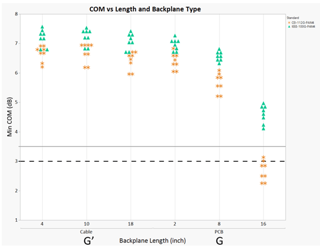
Figure 3: The three models on the left are for cable backplane, and the three on the right use a PCB backplane. Note that the 16-in PCB backplane channels (which had 5-dB insertion loss margin in Figure 2) now have negative margin for COM system level metrics on most 112-Gbps lanes.
We would expect to have less margin with the higher data rates, and that is supported in Figure 3. The cable backplane demonstrates similar COM performance across all three lengths (4, 10, and 18 in.) while the PCB backplane exceeds the ability of the SERDES to compensate for loss, reflections, and crosstalk after 8-in of backplane route length. In addition, for the 8-in and 16-in PCB backplane, note the delta between 100-Gbps and 112-Gbps speeds with the separation in COM results becoming more pronounced. For a 16-in PCB backplane at 112-Gbps PAM, this system has a negative COM, despite having significant margin with respect to the OIF-CEI-112-LR insertion loss limit line.
In the past, a 6-dB margin would be a comfortable place for the designer to stop development and analysis, confident that un-accounted for error terms would be small in comparison. For 112 Gbps and higher, that is no longer the case. It is important to assess channels in regards to end-to-end multi-lane effects at the system level, including all significant regions of interconnect. Connector systems that offer options for both board-to-board and cable-to-board interconnects can be used to navigate the design trade space and also offer significant opportunities for earlier integration and longer sustainment.
Samtec offers connectors and cables to support both PCB and cable backplanes [5]. If you are still wondering: should I use a PCB or cable backplane for a high-speed design? Get more detailed information on this topic, see the full article in Signal Integrity Journal by Andrew Josephson, Brandon Gore, and Jonathan Sprigler of Samtec.
Related Demos
Cable Backplane + META-DX1 Ethernet PHY= Great Performance at 3 Meters, 56 Gbps – The Samtec Blog
PECFF AI Hardware System Architecture With New Cable Backplane – The Samtec Blog
Six New 112 G Connector Systems Is The Coolest Demo At DesignCon (IMHO) – The Samtec Blog
References
- Twinax Product Data, Samtec website
- Simonvich, Bert. “Controlling Electromagnetic Emissions from PCB Edges in Backplanes” Signal Integrity Journal, January 2017.
- CEI-112G-LR-PAM4 Clause 27.2.4, pg 582-597, in OIF-CEI-05.0.
- IEEE 802.3ck taskforce (draft has not yet been published)
- High Speed Backplane Systems, Samtec brochure
Leave a Reply