Samtec’s Gustavo Blando recently presented “Increasing Broadband Interconnect Characterization” at EDI CON 2018 in Santa Clara, California. A video of the workshop is above, and below is Gus’s summary of his presentation.
VNA measurements are the backbone of any SI analysis, both for correlation and basic interconnect understanding. As bit rate increases and specs tighten, accurate measurement at higher frequencies is of paramount importance.
For convenience, a coaxial style connector is often used to interface the DUT. This introduces discontinuities along the signal path that can severely affect the maximum measurement bandwidth. In this work, we study the interface discontinuities that limit bandwidth from the connector to the PCB launch. We propose a PCB launch design pattern that enables measurement up to 60GHz. It also shows how PCB manufacturing variations can dramatically change the effectiveness of measurement bandwidth by utilizing the measurements of CT-Scans and simulations.
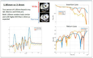
When placing the connectors back-to-back, we can measure and identify the difference between 2.4mm and 1.85mm RF connectors. We can see through VNA measurements why 1.85 mm connectors are rated to higher frequencies. The measurements show the 2.4 mm style connector start losing bandwidth as soon as 35GHz to 40GHz. Conversely, the 1.85 mm style allows bandwidth in excess of 60 GHz.
In addition, we show that not all connector vendors are created equal. The difference between vendors can be tested by placing the connectors back-to-back, and comparing the differences in frequency and time (TDR) domains.
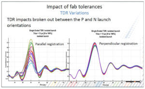
PCB manufacturing registration has an important effect on launch absolute value and symmetry between P and N. Registration in the order of 3 mils between TOP and L1 could result in a launch impedance differences of up to 5 ohms, and will severely limit the bandwidth of the launch.
Finally, we identified special launch structures specifically designed to minimize registration sensitivities. Since we cannot control all manufacturing sensitivities on the PCB, the best route was to try to design launches that take that variation into account, thus improving the launch, even in the presence of such sensitivities.
Other links that may be of interest: