Free Wideband RF Launches White Paper

Samtec recently published a major white paper, “Wideband RF Launches: Much More Than Footprints On PCBs.”
This white paper shows that very wide bandwidth RF launches are possible to implement in PCBs, even with vias included. This does not mean it is a trivial task. Competing requirements, be they electrical, mechanical, manufacturing, or cost, must be considered and balanced simultaneously.
This white paper — a link to it is at the end of this blog — elaborates on some of the most important design considerations. Optimizing these factors requires working with your PCB house to understand those manufacturing limitations. Ultimately, getting to 90-100 GHz bandwidths will, in many cases, require pushing the edge of today’s fabrication limits. Understanding the limits at the start of the design process goes a long way toward reaching a high-performance launch, which ultimately means high-fidelity connections to your device.
The paper begins by defining an RF launch. The launch includes the connector, signal via, and the via to the trace transition inside the PCB.
Four primary topics are discussed:
Section 1: Impact of Via Stubs
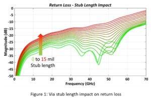
The key takeaways of this section are:
- >8 mil via stub will hinder getting > ~ 60 GHz launch bandwidth
- Fab limits on stub length AND length tolerance will determine launch limits
- Designing-in compensation for the longest stub will make things worse for the shortest stub length. Tight tolerance is critical for wide bandwidth!
Section 2: Correct Ground Ring Sizing
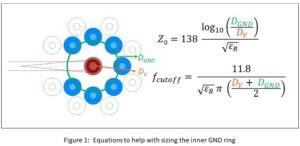
The key takeaways of this section are:
- When designing RF launches with bandwidths >70 GHz, choosing dielectrics with ER<3 and drill diameter ≤ 5 mil is likely necessary for good performance.
- Loss factor is a good metric to see when a launch is no longer behaving as designed.
Section 3: Misregistration Compensation
Key takeaways are:
- A tapered transformation from via to trace lowers the impact of via-to-etch misregistration
- Minimize launch asymmetry between channels to minimize differences in performance
Section 4: Launch Performance Issues Introduced During Connector Assembly
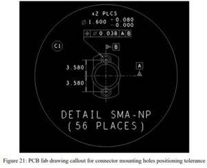
- Use tight hole size and positional tolerance to ease assembly
- Align to copper features to minimize assembly variations
There are many types of RF connectors that are used in different applications. This white paper focuses on compression mount PCB connectors. With the number of high-speed connections in PCBs increasing continually, compression mount connectors provide a number of advantages to meet this demand:
- They are relatively compact, which means a number of them can be placed on a PCB.
- They can be placed anywhere on a PCB. This allows them to be placed close to the device the signal needs to reach.
- They can be reused.
Instantiating them on a PCB and achieving full bandwidth requires careful design. Just like a race car needs the optimal tires that allow it to obtain sufficient traction while going as fast as possible, RF PCB connectors need a good launch structure in order to get the widest bandwidth signal transfer into and out of the PCB.
Here is a link to the “Wideband RF Launches: Much More Than Footprints On PCBs” white paper (it’s free — you’re not required to register to read it). Here’s a blog with frequently asked questions about wideband RF launches. And here’s a link to Samtec’s RF product line.