DesignCon 2018, which is a big deal for Samtec, is a few weeks away. Our high-speed technologies for Silicon-to-Silicon optimization will be on full display and our product experts will show new products that are just released, or will be released in 2018. Our application engineers will demonstrate new system-level solutions, and our SI experts will present technical papers.
In the next few weeks we’ll write about all of these products, demos, events, and presentations. To help you maximize your time at the conference, here’s a schedule of Samtec’s conferences and presentations.
Samtec DesignCon 2018 Featured Events/Demos
Monday, January 29, 2018 | 1:00pm – 5:00pm | Rooms 209/210, Santa Clara Convention Center
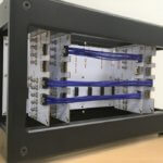
Samtec is proud to sponsor the IEEE P370 Plugfest. Register for this event here.
Thursday, February 1, 2018 | 1:00pm | Ansys, Booth #747
Scott McMorrow, Samtec’s CTO of Signal Integrity Products, will be giving an in-booth presentation on Trailblazing Past 56 Gbps-PAM4 with Samtec Flyover™ solutions.
January 30 – February 1, 2018 | Keysight, Booth #725
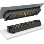
An active 32-port demonstration of Samtec’s Flyover QSFP28 double-density (FQSFP-DD) to ETC6 56 Gbps NRZ slim body cable assembly will be on display throughout the show.
Presentations
Wednesday, January 31, 2018 | 11:00am – 11:45am
Effective Return Loss for 112 G and 56 G PAM4
Room: Ballroom B
Track Name: 04 System Co-Design: Modeling, Simulation, and Measurement Validation Electromagnetic Compatibility/Mitigating Interference
Description: This paper proposes using a pulse echo for time domain reflectometry (TDR) rather the commonly used step function echo. The echoed pulse response of a single symbol is convolved with the modulation signal levels to produce an effective reflection coefficient metric at a specified bit error ratio (BER). A conversion to dB presents effective return loss (ERL) in more familiar return loss units. ERL is a single value which replaces the commonly used frequency domain return loss (RL) masks. It makes RL grading simple, straightforward and meaningful.
Wednesday, January 31, 2018 | 2:00pm – 2:40pm
Designing DC-Blocking Capacitor Transitions to Enable 56 Gbps NRZ & 112 Gbps PAM4
Room: Ballroom F
Track Name: 08 Optimizing High-Speed Serial Design
Description: DC-blocking capacitors are required in almost all applications of high-speed SERDES in order to level shift the differential signal to the optimum operating point for receiver performance and to avoid DC ground loops. As we start the transition from 28 Gbps to 56 Gbps NRZ and 112 Gbps PAM4, it is crucial that the DC-blocking capacitor present a high bandwidth, near-reflectionless transition to the signal in order to maintain at least 32 GHz of effective interconnect bandwidth. In this paper, we discuss the steps necessary to generate a realistic, detailed capacitor model for data transmission and optimize its layout for an electrically transparent design.
Wednesday, January 31, 2018 | 3:45pm – 5:00pm
Panel – The 400G Ethernet Turn: The Rise and Fall of the Eye Diagram
Room: Ballroom F
Track Name: 10 High-Speed Signal Processing, Equalization, and Coding
Description: The eye diagram is the bread-and-butter tool in many areas of digital communication and signaling. It is a straightforward visual gauge of the signal quality. As signaling moves from NRZ to PAM4, from below 10 GBd to 25+ and 50+ GBd, Ethernet and other standards shifted away from eye diagram measurement to linear fitted pulse, SNDR, and other methods. Why this change? We discuss the reasons, the new methods and what worked well and what was difficult, the acceptance and the way forward in 50+ GBd electrical and 100 GBd optical. Then we ask, “Is this transition a general move?” It certainly is occurring differently in different standards, so we compare the very highest speed standards to the latest DDR memory buses.
Thursday, February 1, 2018 | 11:00am – 11:45am
A NIST Traceable PCB Kit for Evaluating the Accuracy of De-Embedding Algorithms and Corresponding Metrics
Room: Ballroom G
Track Name: 13 Applying Test and Measurement Methodology
Description: In this presentation, we will introduce the two de-embedding/fixture removal techniques that have been gaining traction in the industry (2x-Thru and 1x-Reflect) comparing them with other fixture removal techniques. We will then describe a NIST traceable methodology to evaluate the de-embedding accuracy of these techniques for single-ended and coupled differential applications using a series of PCB test coupons. We will also discuss the appropriate metrics needed to evaluate the accuracy of the de-embedding algorithms.
Thursday, February 1, 2018 | 2:50pm – 3:30pm
Improving TDECQ and SNDR for Better Characterization of Serial Data Signals and Path from Mask Test to TDEC, SNDR, and TDECQ Measurements
Room: Ballroom G
Track Name: 09 Measurement, Simulation, and Optimization of Jitter, Noise, and Timing to Minimize Errors
Description: The test of high-speed serial data signals has developed from mask test to TDEC, transmitter and dispersion eye closure. With signaling moving to PAM4, measurements move in two directions: SNDR for PAM4– signal to noise and distortion ratio, a transmitter test tool which sums noise and other non-compensable features into one figure-of-merit number; and the TDECQ, transmitter and dispersion eye closure penalty quaternary. We summarize these developments, and in an original work we show improvements for SNDR and TDECQ for the near future.
Thursday, February 1, 2018 | 3:45pm – 5:00pm
Panel – How to Avoid Getting Totally Skewed: Glass-Weave Skew in High-Speed Design
Room: Ballroom D
Track Name: 08 Optimizing High-Speed Serial Design
Description: The objective of this panel session is to guide design teams through the process of evaluating and selecting the right glass styles or design strategies for eliminating glass-weave skew for multi-gigabit, high-speed PCB designs. Several methods have been proposed, including choosing a glass style that minimizes resin windows, aligning trace direction to the fill/weft, routing each member of the pair at the same pitch as the glass fibers, mechanically spread glass, dual-ply glass, zigzag routing of differential pairs at a 10º angle to the weave, building each PCB with the artwork rotated at a 10º angle to the panel and weave, or using glass with a lower dielectric constant (closer to the resin Dk).
In this panel session, we’ll nail down the answers to this quintessential design concern once and for all – or entertain you while the experts slug it out!
Thursday, February 1, 2018 | 3:45pm – 5:00pm
Panel – 400G Test & Measurement Ready for the New Challenges Ahead
Room: Ballroom C
Track Name: 13 Applying Test and Measurement Methodology
Description: 400 Gbps Ethernet is now close to standardization and we are already seeing successful & exciting results from early field trials. Many of the novel aspects of 400 Gbps Ethernet pose significant test and measurement challenges and this presentation highlights the revolutionary aspects of 400 Gbps technology and how it drives new concepts in test and measurement. From PAM4 modulation in the electrical and optical domain to the challenges of validating margin in FEC based links the presentation explores how the T&M community within the Ethernet Alliance is ready to take 400G to widespread and pain-free deployment.
Passes
Register for your free VIP Expo Pass, or use our Promo Code: guest for 20% off Conference Passes.
Learn more about DesignCon 2018.