“112 Gbps PAM4 data rates will save the world!”
A reader of the Samtec blog may think that. Why? The demand for data never ceases. A recent report says that US teenagers spend seven hours a day in front of screens.
But how real are 112 Gbps PAM4 data rates? Test silicon is available from a few SerDes and FPGA vendors. Production silicon is at least 18 months away. However, 112 Gbps PAM4 data rate system design and testing are already underway.
The SI requirements for next-gen systems can be daunting. So, what is being done to assists engineers faced with these issues?
SI Expertise From Keysight and Samtec
Designing for high-speed data rates (56/112 Gbps PAM4) is not easy. Every design detail needs consideration to optimize performance. This applies equally both in copper and optical domains.
System architecture selections come into play. What is the best path signal path: PCB, cable, fiber? Additonally, the signal channel need state-of-the modeling, simulation, analysis and testing techniques.
Thankfully, Samtec has the system architecture solutions and Keysight is a leader in test and measurement. Samtec and Keysight partner to provide engineers the best of both worlds.
Keysight (and Samtec) offers continuous training on the latest solutions in product and SI techniques. At a recent seminar, Keysight championed a holistic approach to simulation and measurement by reviewing the SI basics with latest hardware and software solutions.
Keysight SI experts and Samtec Product Specialists reviewed the following:
- SI analysis techniques such as mixed-mode S-parameters, eye diagram, time domain reflectometry (TDR) and single pulse response
- Channel to channel crosstalk
- Measurement instrument calibration
- Fixture removal and De-embedding
- Channel modeling, material properties extraction, and channel optimization with measured S-parameters
- Next-gen 112 Gbps PAM4 interconnect test fixtures for mezzanine applications
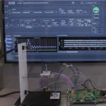
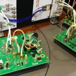
NovaRay™ SI Eval Kit Test Set-up
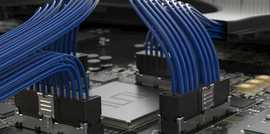
Samtec’s NovaRay™ is an industry-leading high bandwidth, high-density interconnect system. The innovative pin-to-ground differential pair configuration enables:
- Very low crosstalk to 40 GHz+
- Tight impedance control
- Minimal variance in data rate as stack heights increase
For SI geeks, the system is 112 Gbps PAM4 capable. It’s also rated up to 56 Gbps NRZ per channel.
Samtec demonstrated the latest NovaRay™ SI Evaluation Kit at the Keysight event. In the two-PCB system, one PCB contains NVAM series while second contains NVAF series. The kit routes 5x high-speed differential pairs from the NVAM/NVAF connectors to high-precision RF connectors.
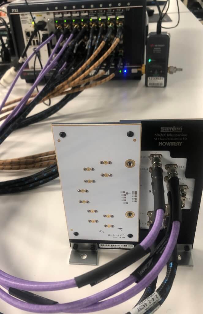
As illustrated, the Samtec kit was attached to a Keysight PXI VNA running Keysight N1930B Physical Layer Test System (PLTS) 2019 Software. What results were achieved?
NovaRay™ SI Eval Kit Test Results
Samtec typically demonstrates new platforms using PBRS31 test patterns. However, the advantage of using Keysight’s PLTS is the variety of protocols can emulates through the DUT.
Fortunately, The Keysight PLTS software offers support for IEEE 802.3bs test pattern generation. It also supports other protocols.
In this instance, a 53.25 Gbps (25.5625 GBd) test pattern was applied the NovaRay SI eval board emulating a portion of a 400 Gbps (8 x 50 Gbps) Ethernet chip to module application.
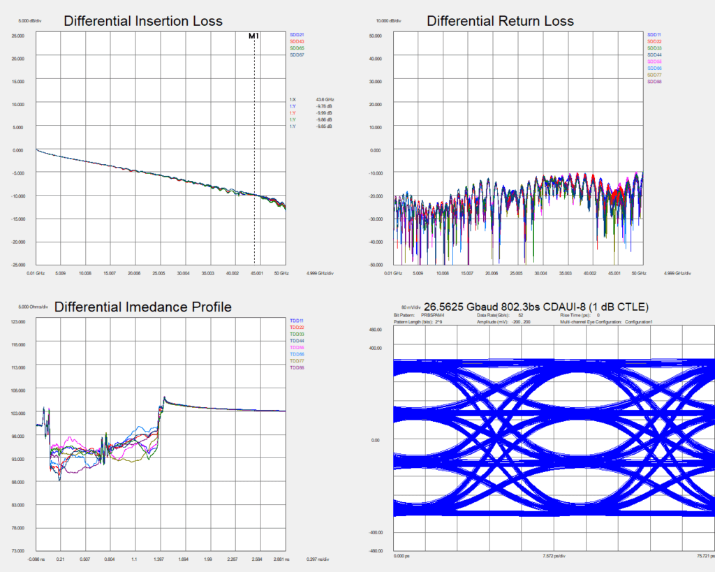
What results were achieved? As illustrated, Differential Insertion Loss was about -12 dB at 50 GHz. The roll-off was very flat, linear and smooth from DC-50 GHz
Also, the Differential Return Loss was around -10 db at 50 GHz. The performance from DC to 50 GHz was roughly flat as well. The eye diagram as was also clean and easily decipherable.
In conclusion, the test results show that NovaRay provide a preferred mezzanine solution for next-gen system design. NovaRay cable solutions also provide system architecture alternatives for bleeding edge performance.
For more information, contact Samtec’s SI experts at [email protected] pr please visit www.samtec.com/novaray.
Leave a Reply