Connector Designs To Address Data Rate and Density Challenges
Demand For High Data Rate
As the need for bandwidth continues to increase, so does the need for higher data rates within a system. What was once one to three Gbps, then moved to 4 to 8 Gbps, and now we are approaching 28 Gbps and looking forward to 56 G. This trend was recently driven home at DesignCon 2018, where many exhibitors were demonstrating interconnects running at 112 Gbps PAM 4.
Although the Datacom and Telecom industries are abuzz pushing these cutting-edge data rates, achieving this performance is much easier said-than-done. Design challenges include routing complexities on the PCB and the potential need for higher layer counts. For longer trace lengths, more exotic PCB materials with lower dielectric constants and re-timers are incorporated to mitigate degrading signal loss. All of these factors add more cost to the system.
Besides materials and costs, designers also frequently face challenges with the decreasing size of the finished products. The proliferation of mobile and hand-held devices drives this trend, as well as new requirements in industries such as telecom, high-power computers, medical devices, aerospace and defense, and even industrial applications.
In addition, new high data rate chipsets, which of course are designed to generate as little heat as possible, still produce heat. These often require more and bigger heat sinks, further complicating the design dilemma.
Obviously, the increasing demand for smaller, higher bandwidth PCBs pushes R&D in the interconnect industry. Sales of both micro pitch and high-speed interconnect systems steadily increase. The interesting caveat is most high-speed interconnects are also micro pitch. But, the smaller the pitch of the interconnect, the more difficult it is to achieve higher bandwidths.
Smaller and tighter pitch interconnect systems introduce a new set of electrical challenges, such as crosstalk and insertion loss. This is primarily due to the proximity of one differential pair to the next, reduced space for routing, and a reduction in grounds pins.
As with many design challenges, there are several ways to address the problem:
PCB Layout
Designers can alleviate some of these conditions by being strategic about their board layout. Well-planned trace design and routings, location of grounds, vias, etc., improve PCB data rates. PCB design strategies are beyond the scope of this article, but numerous tools, resources, and personnel exist to assist in this endeavor. Samtec, for example, has the Signal Integrity Group and Teraspeed Consulting to assist in these matters.
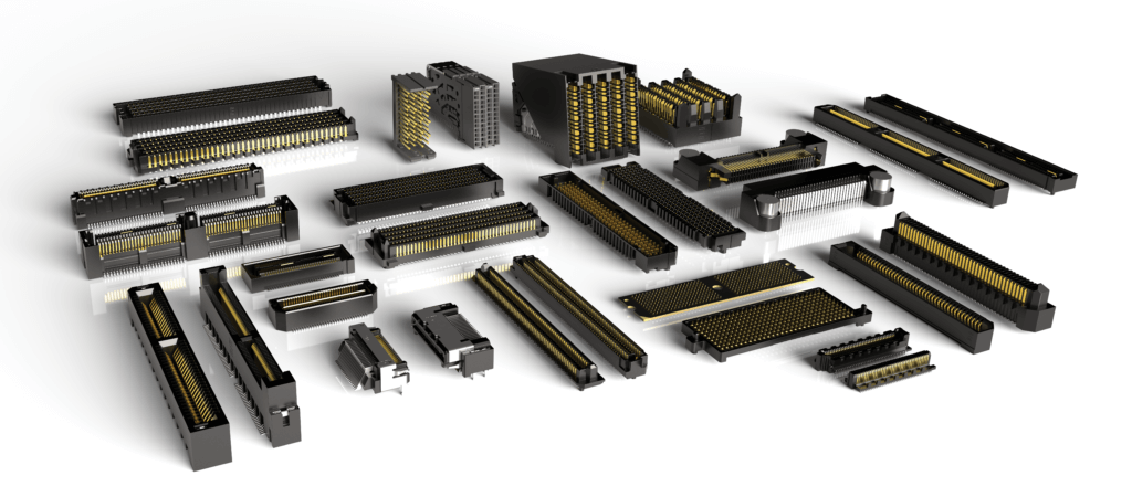
High-Speed, Micro Pitch Interconnect Design
Although the goals of miniaturization and higher data rates conflict, connector manufacturers can strike a balance in performance and footprint size.

One example of these connector design strategies is a contact called Edge Rate®. This contact is designed for higher cycle applications while accommodating higher bandwidths. For example, the .8mm pitch Edge Rate interconnect is rated at 56 Gbps PAM4. One of the ways it achieves this balance between bandwidth and pitch is the design and placement of the pins in the plastic body. Specifically, the thin, narrow, cut edges of the Edge Rage contact are positioned side-by-side. This minimizes the parallel surface areas, which reduces broadside coupling and crosstalk.
Improving Connector Performance
Other connector design strategies to achieve high-bandwidth, micro pitch interconnects include, but are not limited to:
- Perform multiple simulation cycles in the early stages of the design, in order to accurately quantify product performance before you begin the expensive tooling process.
- Minimize the stub in the contact area when the connector is mated. Mechanically, the longer the stub the better for reliability, but the longer stub is an electrical liability acting like an antenna.
- Simplify contact geometry for improved signal path performance.
- Shorten the pin length to minimize the distance the signal must travel.
- Incorporate, where possible, asymmetrical footprints and contacts; alternating designs decrease crosstalk from pair-to-pair within the row of pins and between rows. Said another way, the footprint should drive the connector performance.
- Optimize the connector Break Out Region (BOR). Think of the connector as a critical node in the link; focus not just on the node, but the link.
- Incorporate common ground planes into the connector, space permitting.
- The choice of plastic molding obviously affects connector performance. Among other concerns, we carefully consider the following attributes
- High temperature plastic for RoHS
- Matching Dk for the desired impedance control
- Dimensional stability over temperature and time
The bottom line is, the shorter and straighter the signal path (and connector contact), the better the signal integrity performance. But the balancing act is the connector must have adequate normal force and withdrawal force, as well as have a certain degree of ruggedness. The latter considerations usually detract for the signal integrity performance.
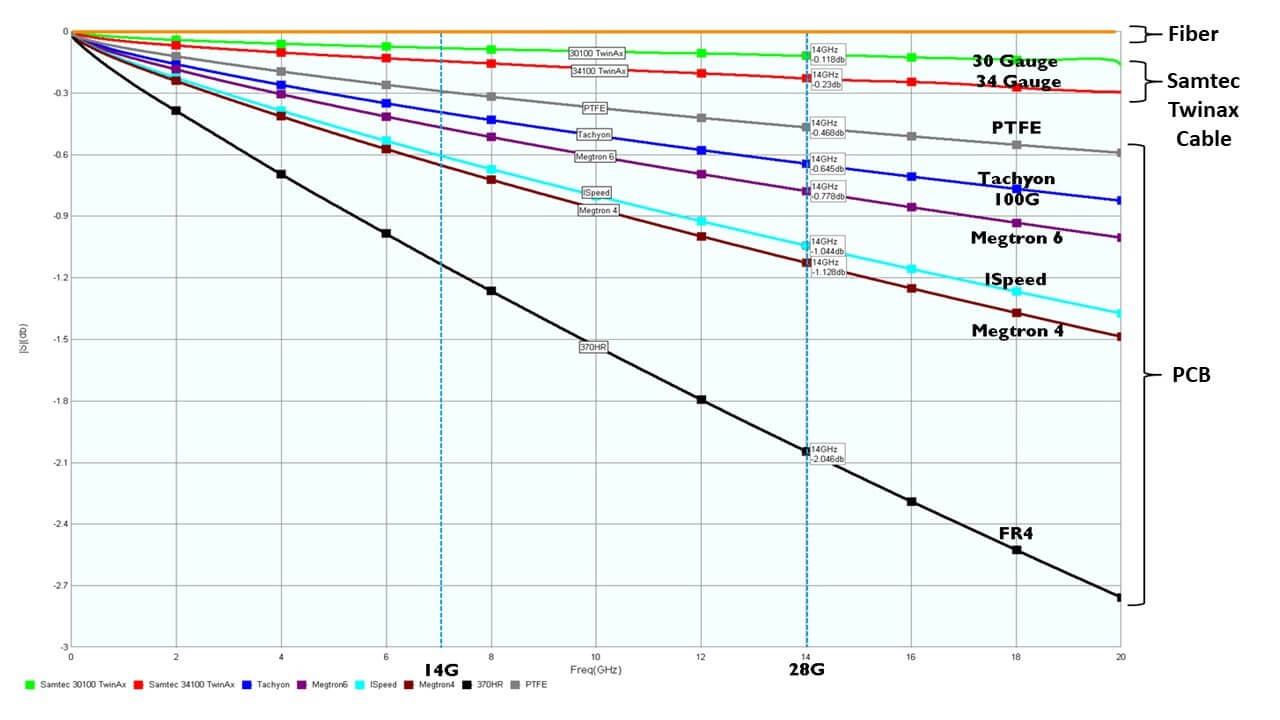
Although the goals of miniaturization and higher data rates conflict, connector manufacturers can strike a balance in data rate performance and footprint size. Interconnect contacts can be designed to minimize size and maximize bandwidth. The plastic materials in the connector insulator also affect performance. And alternative strategies, like taking signals off-board with high-speed cable systems, can address the challenges of speed and cost.
Other links that may be of interest: