Increased density, shrinking footprints, higher data rates, and thermal management are but a few of the challenges affecting the design and fabrication of printed circuit boards (PCBs) in today’s electronic systems. And did I mention cost?
An important, although sometimes overlooked consideration, is these increasingly sophisticated PCBs often require more complex connector systems. Most of the aforementioned design factors also affect connector design and performance, including smaller footprints, diminishing profiles, and the need for increased reliability. And did I mention cost? These strict connector design parameters can create conflicting goals for connector manufacturers, namely balancing the need for increased performance and density while managing costs.
One of the most common connector-related challenges – one that is often not considered until it raises its potentially ugly head – is aligning multiple connector sets between two mated PCBs.
This is a common point of discussion for Samtec Product Engineering and the Interconnect Processing Group (IPG)(1). They have worked with countless Design and Process Engineers on this issue. I spoke with Kevin Meredith, Product Engineer at Samtec, about the challenges of aligning multiple connector sets between two PCBs
Kevin explained that if mezzanine connectors and sufficiently rigid PCBs were fabricated, processed and assembled to exact nominal conditions, then an infinite number of connectors could be successfully deployed between two PCBs. Tolerances and material properties therefore, become the limiting or driving factors.
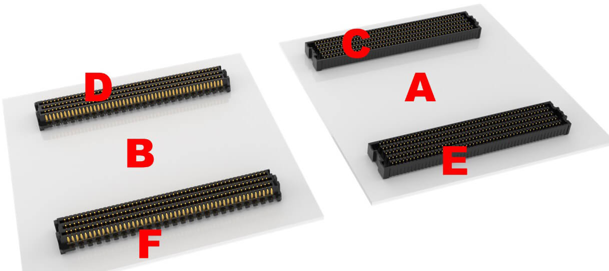
Figure 1 illustrates this point. A multiple mezzanine connector system is an assembly of six components or more: the motherboard (A), a mezzanine card (B), female connector #1, (C), which mates to male connector #1 (D), female connector #2 (E), which mates to male connector #2 (F). Designers need to consider and account for the tolerances of all components, including the often-neglected but relevant tolerances of the two PCBs, (A) and (B).
DANNY: Kevin, what are the effects of adding a second set of mating interconnects to two PCBs?
KEVIN: There are no tolerances to stack for an application with a single mated connector set. In such an application the mezzanine card is assumed to be free-floating and the macro and micro alignment features of the connector will ensure perfect alignment.
However, the addition of other mated connector sets, onto the same mother-mezzanine card, in any direction, at any distance, will introduce several tolerances which will stack. These tolerances are unique to the PCB fab shop, the electronic manufacturing service, and the properties of the materials used in the PCBs.
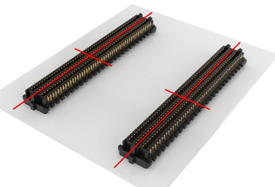
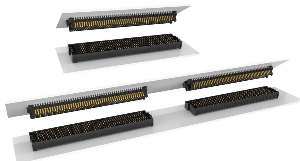
Figure 2 illustrates this point. With one mated connector system (top), the mating socket and terminal strips are free to capture and self-align. But with multiple sets (bottom), the connector centerlines are now fixed relative to each other and subject to additional tolerances.
DANNY: This sounds like it could get complicated. How did we get here?
KEVIN: In one word, “miniaturization.” Connector pitches have decreased from 0.100” (2.54 mm) to 0.016” (0.40 mm) in the last 25 years. That is over a 6X change. Obviously, tolerances must be tightened.
Some PCB purchases are controlled only by the specifications embedded in the Gerber packet. It is possible to build PCBs from these packets without any consideration for mechanical tolerances. For multiple connector applications, separate mechanical drawings must accompany this packet which dictate artwork, drilling and routing tolerances.
DANNY: What is the role of the connector manufacturer in this process?
KEVIN: Looking back at Figure 1 as an example, the multi-connector mezzanine card system will be composed of components A-F. The connector manufacturer only controls the tolerances of the connectors. The precision level of the PCBs and their processing is beyond the control of the connector manufacturer.
Speaking only for Samtec, our goal is to ensure that our connectors meet or exceed published performance specifications. To assist in this endeavor, we make PCB tolerance and processing recommendations. We will even provide referrals for PCB suppliers and equipment recommendations, as needed.
All Samtec products are supported by footprints and product specifications. The information contained in these documents will allow the final equipment designer to complete the system level tolerance study needed to successfully use multiple connectors between the same card.
DANNY: How do you set limits to ensure the proper functioning of the connector set in these types of applications?
KEVIN: The connector system will function properly as long as the initial and final, and angular and linear misalignments are not exceeded. Exceeding the misalignment values could result in open or damaged circuits and/or insulators.
Samtec calculates these misalignment values by taking into consideration factors such as insulator interference, beam deflection, and contact wipe.
I can’t emphasize how important it is for designers to perform a system tolerance study to determine the connector misalignment generated by their design, and then compare those results to the connector manufacturer’s misalignment specifications.
We frequently work with designers to verify misalignment tolerance stacks, but they usually have all of the necessary information at their fingertips because they know their design, component tolerances, equipment, and manufacturing capabilities.
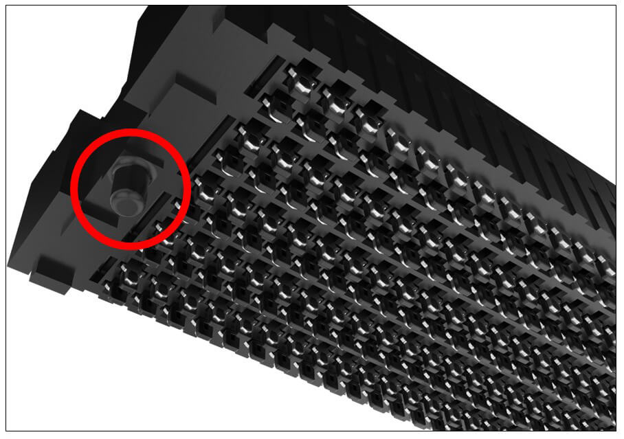
DANNY: Some connector manufacturers offer optional alignment pins, usually located on opposite sides of the bottom of the connector. Do you recommend the use of alignment pins?
KEVIN: Alignment pins assist in hand placement, and can be used to polarize the connector to the PCB. For single connector applications they do not contribute to the overall tolerance stack.
For multiple connector applications they can contribute to the overall tolerance stack. We recommend using connector products without alignment pins. But, if PCB polarization is desired, we recommend drilling over-sized holes in the PCB and then machine-placing.
Our general approach for aligning multiple connector sets is to datum all solder pads from position A1 in solder pad array A. We then look to precision-place the connectors on the pads prior to reflow.
Adding fixturing or dowels to assist in connector placement often reduces the overall precision of final connector placement relative to one another. These methodologies often rely on a drilled hole in the PCB relative to the artwork. The positional tolerance of this hole is typically poor, so Samtec advises against using fixturing or dowels.
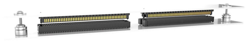
DANNY: What are your recommendations when it comes to using jack screws to secure the two PCBs?
KEVIN: We recommend placing jack screws as closely as possible to the connector system. This will localize stress to the vicinity of the connector and decrease the unsupported PCB span. Increased spans will induce bending stresses in the PCB that could have detrimental effect on other surface mounted components.
DANNY: Speaking of stresses, what about PCB loading?
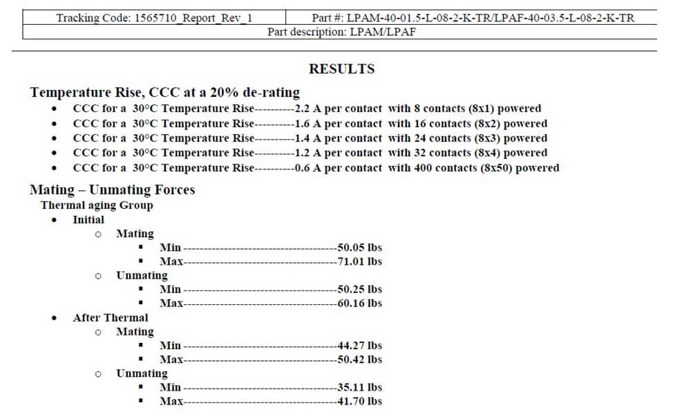
KEVIN: Do not neglect your PCB loading. Always confirm connector mating and un-mating forces, as found in the product qualification test reports. Figure 4 is an example of the mating and un-mating forces presented in a typical qualification report. A significant number of I/O’s can result in extremely large forces. These forces can cause excessive deflections in the PCB to the point that additional stiffeners are required to support the PCBs.
DANNY: Kevin, thanks for sharing. How do you summarize all of this?
KEVIN: Aligning multiple connector sets between two PCBs is possible. Be sure to perform a system tolerance study to determine the connector misalignment generated by your design, follow Samtec’s recommended footprint and stencil design, ensure a good solder paste print, machine place components, and then compare those results to the connector manufacturer’s misalignment specifications. Here’s a link where you can find other best practices for aligning multiple connector sets.
And here’s another blog about the challenges of aligning multiple connector sets between two PCBs.
If you have questions please contact the Interconnect Processing Group at [email protected].
(1) The Interconnect Processing Group (IPG) is an in-house staff of Engineers who assist our customers to improve the overall processing and manufacturability of their boards as well as helping lower its total applied cost.
Leave a Reply