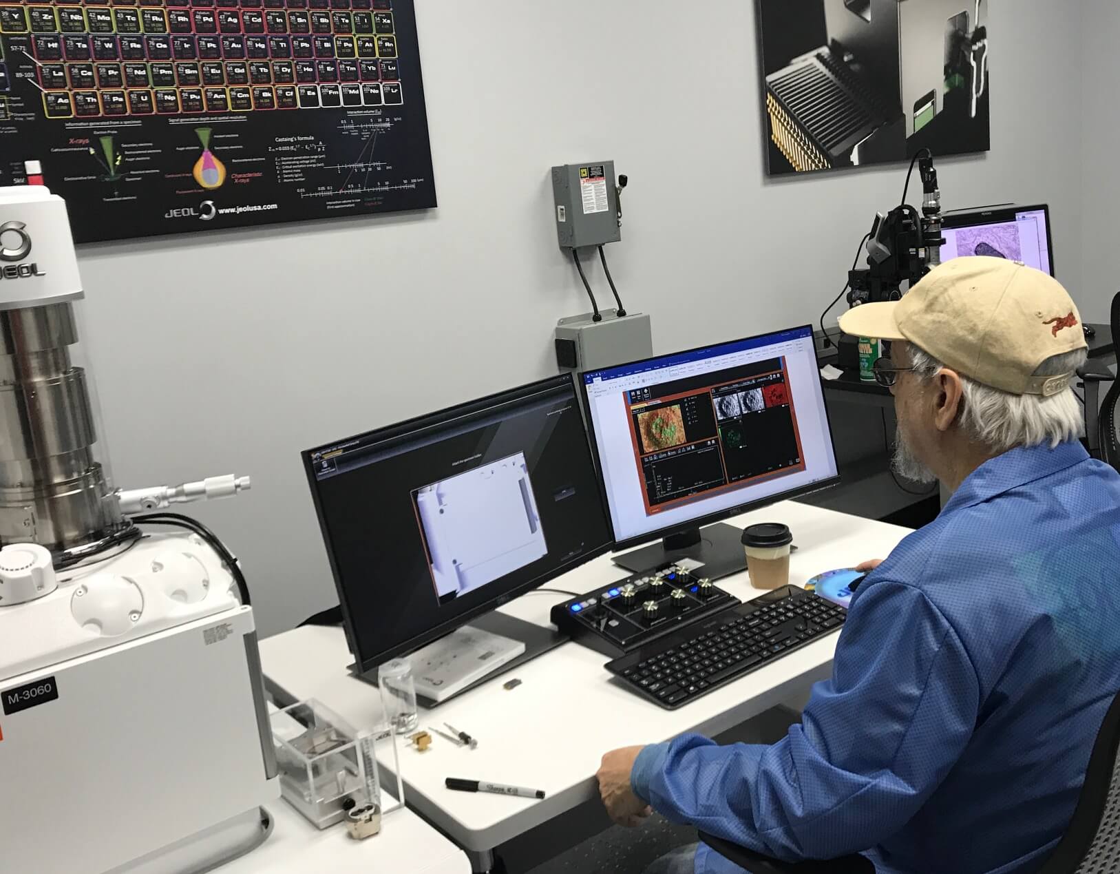
Samtec is one of the fortunate connector companies to own a Scanning Electron Microscope (SEM). We recently upgraded our SEM to a new Jeol, JSM-IT500, which has a 100,000 X magnification power.
I spoke with Dave Scopelliti, our Test, Measurement, and Processing Guru, about this new equipment and how Samtec uses the SEM to improve the quality of our connector products and services.
Danny: Dave, how does a connector manufacturer like Samtec use an Electron Microscope?
Dave: It’s used in a variety of ways, some of the bigger ones being to verify plating thicknesses, solderability, and materials, it helps locate contaminants on contact surfaces, and it’s used for wear analysis, to name just a few.
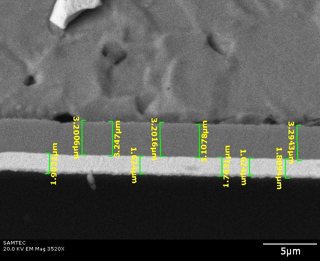
Danny: Talk to me about how the Scanning Electron Microsope is used to verify plating thicknesses.
Dave: The SEM measures plating thicknesses from a profile view (cross sectioned). Connector pins, especially socket contacts (i.e., receptacles), often incorporate geometries which can be difficult to measure with X-Ray Fluorescence (XRF). XRF essentially measures a reflection, which can make it difficult to locate the right tangent for measurement. Also, XRF often provides a reading that is lower than the actual value.
Danny: How does a SEM verify solderability?
Dave: The SEM allows us to inspect the solder joint with much more precise imaging. Of course we focus on the solderability of the connector termination, but we can also evaluate the pcb if necessary. On the pin solder joint, we see the copper, nickel, and the solder joint, and most importantly, we see the intermetallic, which is the physical bond between the materials. This type of clarity is especially important for lead-free solder joints.
Danny: Any examples you can share of how the SEM is used in the product development process?
Dave: It was used recently to differentiate between the conductive plastic and the non-conductive plastic in a subassembly. The SEM showed a location where the conductive plastic was not completely filling the intended cavity in a non-conductive subassembly. Correcting this issue improved the electrical performance of the connector.
Danny: Talk to me about how the SEM is used for wear analysis.
Dave: We use the SEM in the verification testing of our new products. Specifically, it is used to measure the physical wear condition of the mating surfaces. We receive precise measurements of the wear of gold, nickel, and copper at set numbers of cycles (e.g., 100, 200, 500, 1,000 cycles, etc.).

Other Comments From Dave: We can also look for contamination on the contact surface. All of our images are grey scale; the higher the atomic number, the brighter the appearance on the grey scale image. It’s much more difficult to find contaminants on plastics because hydrocarbons (which constitute most of our found contaminants) look very similar to plastic on the SEM. Another limitation is we can’t see the four lowest (lightest) elements: hydrogen, helium, lithium, and beryllium. Our analysis starts with boron, element #5.
Sample preparation and handling is critical so the samples are not contaminated or damaged. Here is a list of SEM submission guidelines, which gives customers specific instructions on what to do and not to do.