Many factors affect the quality and performance of a connector: pin material, the quality
of the stamping, the quality of and choice of surface finish, and the tolerances on the
plastic insulator, just to name a few. Beyond the connector, another factor that is crucial
to the performance of the connector on the printed circuit board is the quality of the
solder joints.
This document addresses some of the most frequently asked questions about
connector solder joints, as answered by David Decker, the Manager of Samtec
Interconnect Processing Group (IPG).
The goal in answering these questions is to provide a brief answer that addresses the
main issue (IOW, it’s not a white paper) …
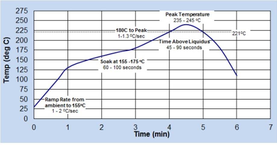
At what peak temperature are most SMT ovens run?
DD: This is probably the most commonly asked question we receive in IPG. The answer is always the same: the peak temperature is the derivative of the solder paste that you use. Our SMT and SMT-compatible through-hole connectors can handle 260° C with no problems. Having said that, most of our customers run their ovens at significantly lower temperatures, usually between 235° and 245° C, for a lead-free profile.
The reason most of them moderate their temperature is to make sure they are not damaging other heat-sensitive components. So when we are asked that question – what is the peak temperature for SMT oven processing — our answer is to consult the solder paste manufacturer and see what they recommend for their specific paste.
Will my solder paste work with Samtec connectors?
DD: The answer is probably yes. Our connectors are widely used, and there are many solder paste manufacturers. We use Alpha solder pastes, which are ubiquitous. Specifically, Samtec uses the following Alpha solder pastes:
- SAC (lead-free)
- WS-820 (Water Soluble)
- OM-338 PT (No Clean)
- Tin-Lead
- WS-809 (Water Soluble)
- OM-5100 (No Clean)
We have many customers using many different pastes, and we try to make all of our connector devices as robust as possible, so that the connector is not the gating item in your processing endeavors. So again, the answer is yes, your solder paste will work with Samtec connectors, with very few exceptions.
Are there any new soldering materials that are gaining interest?
DD: We see a lot of interest in low-temperature solder paste. Of course, lead-free technology requires higher temperature processing. The melting point of most SAC lead-free solder pastes is about 217° C, and that’s up from approximately 183° C for tin-lead solder paste. That’s a significant jump in paste melting temperature. With that delta, from tin-lead temperatures to lead-free, many customers are concerned about component warpage, and potential discoloration of heat-sensitive devices and platings.
Solder paste manufacturers are working on other chemistries and technologies to lower the processing temperature. The ones we see the most with regard to lowering that melting temperature contain bismuth or indium. These new pastes can lower the melting temperature to 140° C. And we know that every benefit has a disadvantage, and the primary disadvantage with these low-temperature pastes is brittle, less robust solder joints.
In my opinion, there’s still some work to be done by these solder paste manufacturers.
Should I pre-bake my components prior to soldering?
DD: Samtec connectors, and SMT connectors in particular, do not require pre-baking. Per IPC/JEDEC J-STD-020E, our connectors do not require pre-baking because the moisture sensitivity level of our connectors is 1. Some customers do decide to pre-bake, and it’s not going to hurt the connectors. The need for pre-baking is because of entrapped water in the device or component; pre-baking evaporates any trapped water content in that device/component.
Pre-baking might be more of a concern if your inventory or manufacturing facility is located in a place with higher humidity levels.
If a connector coplanarity spec is .006”, what stencil thickness should I use for the best solder joints?
DD: This is another question that we are asked just about every day. A connector coplanarity specification of .006” (0.15 mm) is common for bigger connectors (for example, on .100″ pitch, with 15 or more pins). It makes sense to think that the stencil has to be as thick as the coplanarity spec. At the same time, other devices on the same board may require a thinner stencil, for example, .004” (0.10 mm). It’s possible that using a thicker stencil could lead to other problems, like solder joints bridging.
At Samtec, IPG works with the connector designers in the new product development process. When we begin testing the soldering process, we use a .004”, .005” and .006” thick stencil, and we use varying aperture designs, to optimize the stencil design. So our stencil recommendation has been fully vetted, and we know what works and what doesn’t work, for the most part. Unless it fails in our testing, a .004” stencil can be used. And likewise, rarely does a .006” stencil not work. We have stencil thickness recommendations on the product pages of our website (here’s an example). All of the details of these recommendations have been tested and can be trusted.
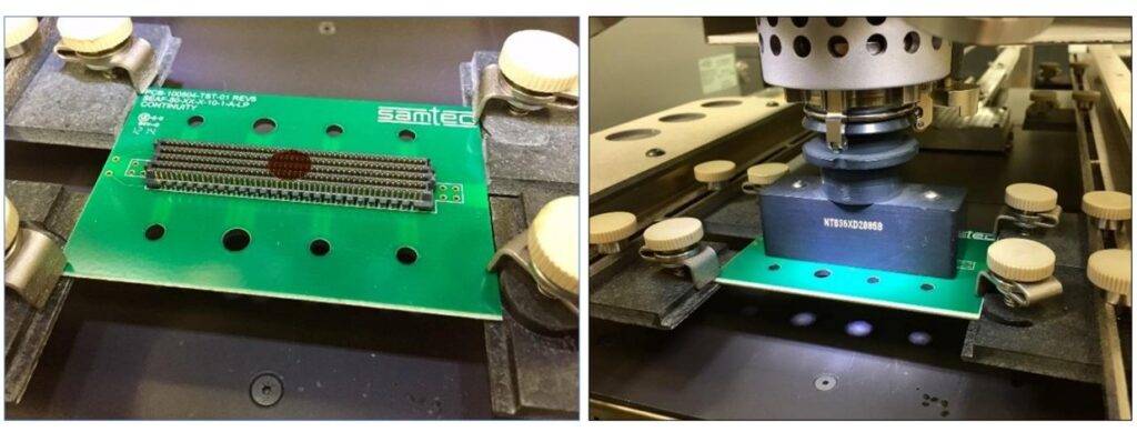
We recently completed a solder joint study with Phoenix Contact about using solder stencils on connectors that are thinner than the connector’s coplanarity spec. This study shows you can successfully solder connectors with a .006” (.15 mm) coplanarity spec using a .004” (.10 mm) thick stencil. A customer might have to do this because they have other devices that require a .004” thick stencil, or because they don’t have the time or budget to handle the expense of using a stepped stencil.
In this study, we designed the stencil apertures to be bigger than the pads on the PCB (i.e., overprinting). The solder that’s printed beyond the pad in all four directions will coalesce and flow back onto the pad and lead during the reflow process. We didn’t experience solderballing or other problems.
What are common problems with two reflow oven passes and inverted components?
This is a common question because this is a common processing method. Our connectors are typically some of the smaller components on a PCB and therefore are typically lightweight. Usually, PCB-level components are on side one of the PCB; the paste gets printed, the components are placed, and the board is run through the oven.
After this pass, the board is inverted – meaning our connectors are now upside down. The larger devices and the heat-sensitive components are usually placed on side two, and the board goes through the oven the second time. So, our connectors go through two oven passes, and they are inverted on the second pass. Most customers are able to process almost all Samtec connectors in this manner, with no problems.
As part of our product qualification testing, we send our connectors through the oven three times: once on a standard soldering pass, and then twice on inverted passes. Almost all of our connectors pass these tests because almost all of our products are small and symmetrical, so the surface tension of the molten solder will hold the connector to the PCB while it’s inverted, without the need for additional hold-downs, locking features, or glue. Connectors that are more challenging are generally larger with an offset center of gravity.
Are the common board processing problems experienced in recent years different from those of 10-20 years ago?
The short answer is yes, primarily due to miniaturization. Components are getting smaller, stencils are getting thinner, and designers are trying to squeeze more parts on smaller boards. All of this adds up to processing challenges.
But, stencil design technology continues to improve, solder pastes are getting better, and reflow ovens are more precise and reliable. In other words, the tools used to create and inspect solder joints seem to be keeping pace with the demand for miniaturization.
What do the different IPC solder joint classes mean?
IPC, the Institute for Interconnecting and Packaging Electronic Circuits, is the recognized governing body for the inspection of solder joints in electronic assemblies. IPC separates solder joints into three classes.
Class 1 is for “General Electronic Products,” meaning if these products fail, it’s a nuisance to the user or they experience an inconvenience. Children’s games and toys are an example of products with Class 1 solder joints.
Class 2, or “Dedicated Service Electronic Products,” is a significant step up in terms of functionality and reliability. If this product fails, the user’s inconvenience and “annoyance factor” is much greater than Class 1, but the user does not face physical harm. Samtec connectors are IPC Class 2.
Class 3, or “High Performance/Harsh Environment Electronic Products,” refers to high-reliability products where performance is critical. Examples include military, aerospace, and medical applications. If these solder joints fail a person might be injured or even killed. A significant number of Samtec connectors are rated IPC Class 3.
An IPC Class 3 rating doesn’t mean every time an EOEM solders a connector they achieve a Class 3 solder joint. Other factors come into play, such as stencil thickness, the precision of the connector placement, and pad design, to name a few.
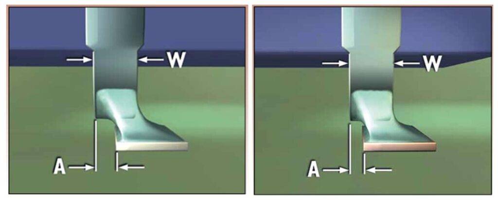
The illustration above shows the difference between a Class 2 vs. Class 3 solder joint. Dimension W is the width of the component lead, and dimension A is how much of the lead is extending over the solder joint/PCB pad. For Class 2 solder joints, A can be one-half of W. In other words, 50% of the lead can be “off” of the side of the pad. For a Class 3 joint, A can only be 25% of the width of W. This is just one quick example that illustrates the differences between Class 2 and Class 3 solder joints. Here’s a link to learn more about the differences between Class 2 vs. Class 3 solder joints.
Do I need to do anything special if I am conformally coating my PCBA?
Conformal coating is a common practice. One of the biggest challenges in preparing a PCB for conformal coating is to protect the contact surfaces, which are typically internal to a socket strip connector, but not always. Also of concern are exposed terminal strip pins for an unshrouded connector.
Masking becomes important in these applications. Here’s a link to a document that discusses several of the more commonly used methods of applying conformal coating as well as masking methods.
Parylene conformal coating is popular. This is a complex process that requires significant masking. The Parylene process involves taking the PCB assembly and placing it into a chamber where a vacuum is pulled. As the vacuum is pulled, the Parylene coating is introduced into the chamber and it goes everywhere air can go, allowing the Parylene to get into every nook and cranny of the connector(s). As you can imagine, it’s very difficult to mask all of the critical areas. If a customer asks us about the Parylene process, we refer them back to the Parylene manufacturer.
If there is a solder joint problem with an array connector, how do I rework it?
As the name implies, array connectors are larger and they typically have an X, Y grid of positions. Samtec grid array connectors frequently have 500 or more I/Os on a single connector. If an internal solder joint on an array connector has a problem – and the vast majority of solder joints on an array connector are internal/under the insulator – your only recourse is to remove that connector and replace it with a new one.
Simply described, the process involves placing the PCB into a hot air rework station. A nozzle is placed on the top of the PCB, just above the surface, but surrounding the connector. A prescribed thermal profile is executed where hot air is introduced around the array connector, the solder melts, the nozzle is lifted off the PCB, and the connector is literally removed from the board using pliers or tweezers.
The board will need to be cleaned and the old solder removed. Our Air-Vac rework system blows hot air on the solder to keep it molten, and a nozzle removes the solder. Once the solder is removed, the rest of the PCB is cleaned. Then, using a mini-stencil, fresh solder paste is printed on that PCB. A new connector is placed on the PCB, the hot air nozzle is placed over the connector, and a profile is run to resolder the new connector. Although it sounds complex, this process works very well.
Samtec recommends maintaining an approximately 1/8” (3.175 mm) “keep out area” around the connector to leave room for this rework system, on the slim chance it’s needed. Here’s a link to learn more about this process.
What is the benefit of using an inert gas reflow oven environment? Does this improve the strength of the connector solder joints?
The term “inert” usually refers to nitrogen gas, which can be infused into a reflow environment to displace oxygen. This minimizes the opportunity for oxidation because oxygen promotes oxidation. The oxygen corrodes and forms a “skin” over the solderable surfaces and the solder itself, which inhibits wetting.
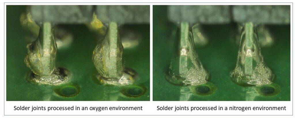
The pictures above show connector leads from an array connector that were reflowed in an oxygen environment (left) and a nitrogen environment (right). The solder joints on the right wet better and are more uniform, and they are simply brighter. All of this is because oxygen was not present.
If you have the opportunity, and if the economics allow, we encourage the use of nitrogen in the reflow process. Samtec tests all of our new products in both oxygen and nitrogen environments.
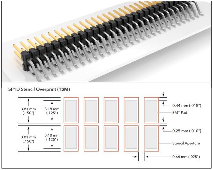
What are the pros and cons of using paste-in-hole (PIH) technology?
Paste-in-hole (PIH) technology has been around for years, and it’s becoming more popular as the miniaturization of PCBs proliferates. If the majority of the components on the PCB are SMT, with the balance being through-hole (TH), it’s possible to process the TH components at the same time as the SMT components.
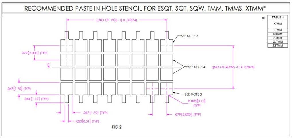
This is accomplished by printing solder paste over the entire PCB, including the plated through holes (PTH) which are used with the TH components. Some of that solder paste will go into the PTH, and some will go around the PTH. Notice the large, square apertures in the recommended stencil design above. The TH components are placed in the same manner as the SMT components; this is possible because of the precision of today’s pick-and-place equipment.
With PIH, all components are placed on the PCB and sent through the reflow oven. The solder paste that is in and around the PTH flows into it, forming a strong solder joint. This reduces your processing steps from two to one.
Designers must make sure the materials in the TH connector can withstand the elevated temperatures of the reflow process and that there is room to print the solder paste on the PCB so that the connector doesn’t sit in the wet solder paste. The latter is typically accomplished through plastic standoffs on the connector. Of course, of most interest is the type of plastic used in the connector body or insulator. Here’s a blog with more information about Paste-In-Hole Reflow Processing.
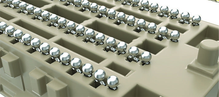
Do connectors self-center during the reflow process?
Don’t I wish! That would solve a lot of problems, especially in applications with multiple connectors on the PCB. But the answer is, in general, no. Flat gull-wing or J-style leads simply don’t have the self-centering capabilities of solder ball products.
Solder wants to reside in the most stress-free geometry, which is a sphere. Solder is most at rest, or stress-free if it is spherical (or ball) shaped. When the entire connector is resting on a solder sphere or ball, and on solder paste that contributes to the size of that ball after it reflows, it does a much better job of self-centering. The video above demonstrates this. The connector with the solder ball leads is intentionally offset about half the pad width, and as the solder reflows, it pulls the connector over the center of the pad. Please note this is a short video; we suggest watching it several times.
What is solder charge technology?
We always want to get more solder in the solder joint. This can be accomplished by printing more paste on the PCB, or you can attach solder to the lead (i.e., a solder-bearing lead), and that’s what solder charge technology is. It’s a clag of pure solder, no flux, that is mechanically attached to the tail lead of the connector. For example, our SEARAY™ product line uses solder charge technology. Solder charges allow you to place more solder in the joint area to form a more robust solder joint.
A loop in the connector contact tail helps hold the solder charge to the lead. The video above illustrates this process.
As mentioned above, the only flux with solder charge technology is what’s in the solder paste. Therefore, it is critical that customers follow our stencil recommendation guidelines, that the connector is properly placed on the PCB, and that sufficient solder paste is placed on the PCB.
More on Solder Joints and Soldering …
If you have any questions please contact the Interconnect Processing Group.
IPG has tons of experience helping customers solve their processing and design challenges. We understand that every design is different and has its own unique issues. IPG can assist you in improving the overall processing and manufacturability of your board as well as helping lower its total applied cost.