Glass; Not Your Mom’s Substrate.
In the days of old we looked into the “green” for guidance on how much further down into the world of miniaturization we could go. What is the green you ask? I am talking about the substrate that has served us all well for many years; the PCB.
We are at a crossroads in the world of substrates, and honestly we are at a point where we need something new, a different way of addressing miniaturization and higher speeds.
What are my options?
The printed circuit board has come a long way from its beginnings, and perhaps can be taken to new highs (or lows in this case) through new materials compositions.
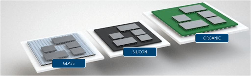
However, if we are honest with ourselves we know that the PCB isn’t the best option for miniaturization. After the PCB came the silicon wafer for use as a substrate.
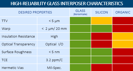
The silicon wafer has the benefit of being able to take vias down to 10 µm, and is considered to be a mature substrate. However, it doesn’t have the electrical benefits of glass since it is a semiconductor where glass is an insulator. Silicon also falls a little short on maintaining a flat surface finish so 2.5D and 3D packaging can become difficult.
Why is Glass a Better Substrate?
To boil everything down in one statement, glass can go smaller than PCB and has better electrical, optical, and flatness properties over silicon. This goes without mentioning that glass is implantable in the human body, and can handle 2.5D and 3D packaging methods with ease.
On top of that, glass can have microstructures etched into, microchannels for fluid transfer and electronics cooling, and can even be used in RF MEMS applications.
Samtec is leading the way in the glass substrate market by offering multiple via types, and multiple materials (Borosilicate and Fused Silica) for varying applications. Glass isn’t finished there, it can be stacked to hermetically seal a package, implanted, and can have channels made to fit any need.
Want to learn more about Samtec’s Glass Core Technology? Check out www.samtec.com/gct and see the GCT video here.