Fan-Out Wafer-Level Packaging
Advances in packaging have afforded companies the ability to place a larger number of contacts in smaller footprints, improve the thermal characteristics, and improve the electrical performance of their systems.
One of these advances comes in the form of Fan-Out Wafer-Level Packaging (FOWLP). FOWLP offers an improvement over wafer-level packaging (WLP), and was developed to provide a greater number of external contacts with a silicon die.
How does it work?
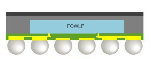
The FOWLP is a more robust method of manufacturing, and removes the size constraints of a normal die. It also affords the manufacturer a larger number of connections between the package and the application board.
FOWLP takes a full silicon or glass wafer and dices it into chips. The good chips are embedded into a low cost material such as an epoxy mold compound.
From there a seed layer can be placed on the glass or silicon and the Redistribution Layer (RDL) can be applied. The advantage of FOWLP is found in “fanning-out” the RDL from under the chip, and giving more room to attach solder balls. See the image at the top of the page for the visual demonstration.
Glass Fan-Out Wafer-Level Packaging
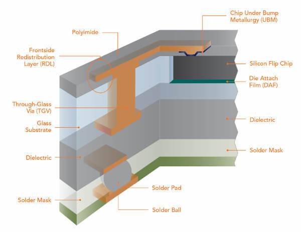
Samtec’s Glass Core Technology (GCT) offers an alternative solution to expensive and limited silicon wafers. GCT leverages the benefits of glass, over silicon, to allow smaller diameter vias and a smaller pitch from via to via.
Samtec offers many solutions with glass packaging. The image below is an example of FOWLP where the silicon flip chip is embedded into the glass substrate, and the RDL fans out over the chip to a through-glass via.
Make sure to check out the first blog we posted on this topic here. A general overview of 2D, 2.5D and 3D packaging was given, and it laid the basis of packaging technology.
For more information on GCT, please visit our Glass Core Technology page, and make sure to check out our latest GCT video here.