
We just started our next round of gEEk® spEEk online seminars. gEEk spEEk is a series of free online seminars covering a wide-range of SI-related topics, all commercial-free.
Stefaan Sercu, Samtec Signal Integrity R&D Engineer, recently presented “Impedance Corrected De-Embedding,” which discussed the advantages of impedance corrected de-embedding over standard 2X through de-embedding.
I spoke to Stefaan about the main take-aways of his popular gEEk spEEk topic. Here’s what he had to say:
DANNY: Stefaan, why did you select this topic?
STEFAAN: As a high-speed interconnect supplier, it is extremely important that Samtec present measurement results that are accurate, reliable and of good quality. Many of our customers use these results to decide if a certain connector can be used in their next generation system. Impedance corrected de-embedding is a method that helps to achieve this requirement.
DANNY: What exactly is impedance corrected de-embedding?
STEFAAN: Before I explain impedance corrected de-embedding, first I need to explain test-board de-embedding.
When characterizing a new high-speed connector, we mount it on a test fixture, typically a PCB terminated with a coaxial launch connector. As a result, we’re measuring not only the performance of the connector but also the performance of the test-boards. These test board measurements are unwanted, since the objective is to measure the performance of the connector only. To remove the impact of the test boards, a model for the test-fixture is required. Once this model is available it can be de-embedded, or you might says it’s “subtracted” from the original measurements. To obtain the test-fixture model, typically a 2x calibration trace is bifurcated. This is illustrated on the figures below:
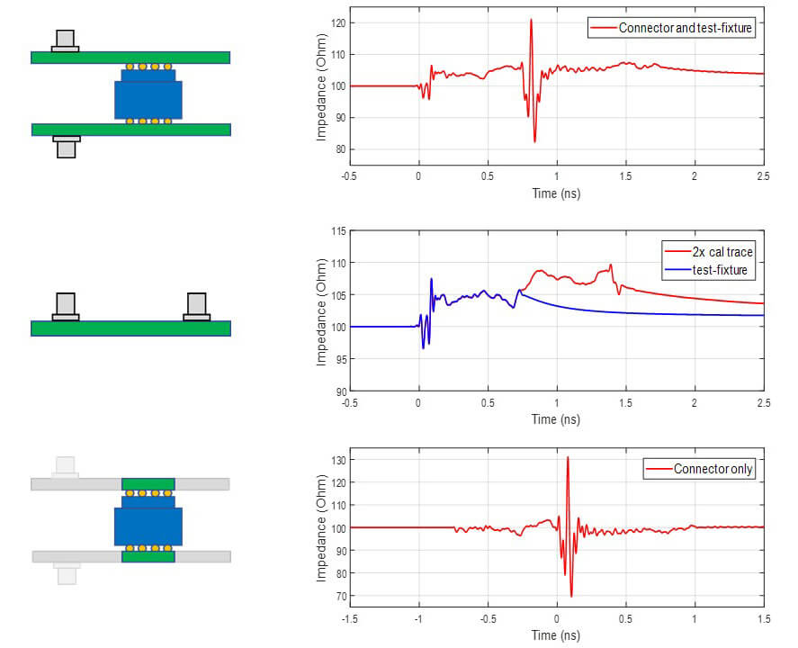
DANNY: The bottom figure shows the impedance of the connector only after test-board de-embedding. This impedance is clearly not causal.
STEFAAN: Exactly, this is the main problem of standard de-embedding methods. A 2x calibration trace is used to derive a model for the test-fixture. Meaning the PCB used to generate the test-fixture model is physically different from the test-fixture PCB. And due to PCB manufacturing process and material variations (e.g., fiber weave effect), the impedance of the test-fixture model differs from the actual test-fixture impedance.
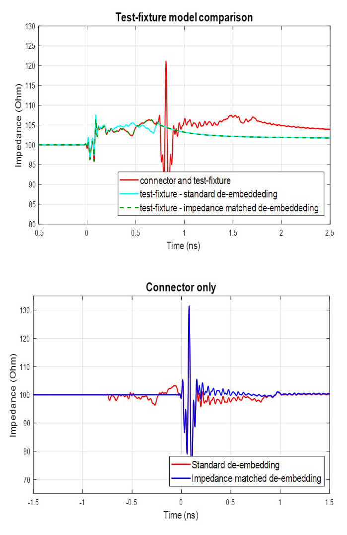
This is the main difference with impedance corrected de-embedding methods. They also make use of the actual test-fixture PCB to generate the test-fixture model and as such, as is shown on the figure below, the impedance of the test-fixture model perfectly matches the impedance of the actual test-fixture. After de-embedding of this test-fixture model, a perfect causal connector only model is obtained.
DANNY: Is it possible to quantify the accuracy improvement that is obtained by using an impedance corrected de-embedding method?
STEFAAN: Well, the achieved improvement depends on the impedance variation between the impedance of the 2x calibration trace and the impedance of the test-fixture. The greater the mismatch, the greater the improvement will be.
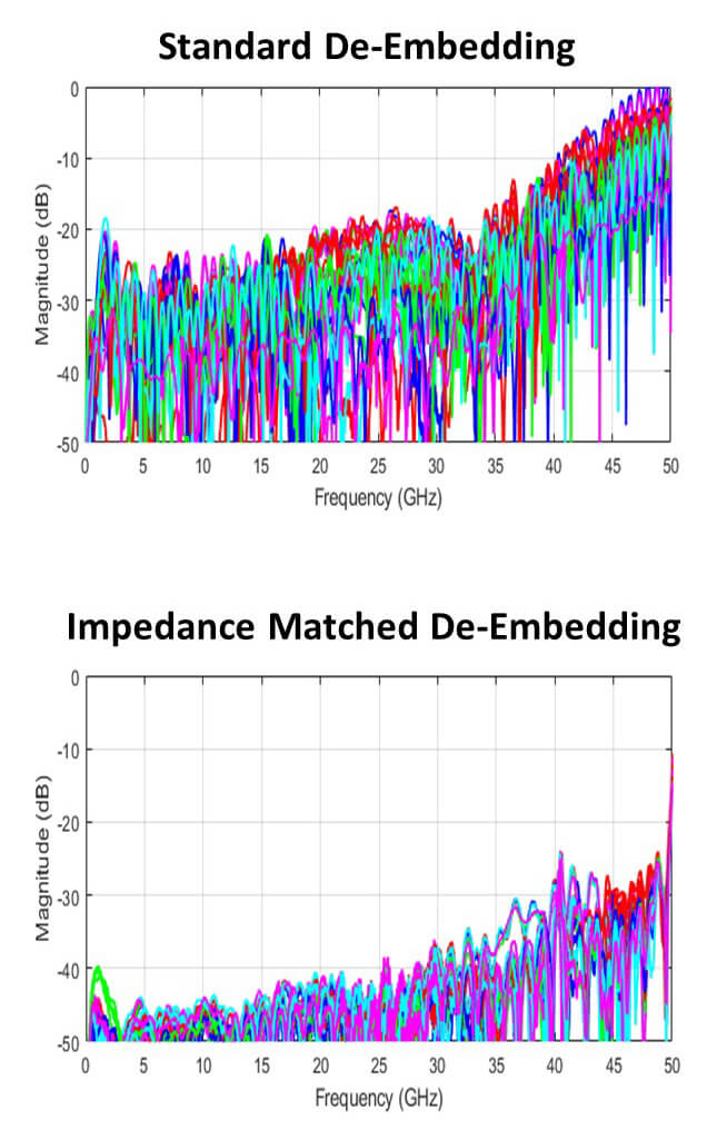
The figures below show the results of a simple experiment. A perfect thru is measured multiple times with various test-fixtures. If no test-fixture would be used, a return loss of about -60 to -100 dB would be measured, depending on the network analyzer settings. Using a standard de-embedding method, the measured return loss is about -20 dB, while using an impedance matched de-embedding method, the measured return loss is closer to -40 dB. A 20 dB improvement is obtained.
DANNY: This blog of course only discusses a few highlights of Stefaan’s presentation. Click here to view the entire Impedance Corrected De-Embedding webinar. Click here to view the slides only.
Other links that may be of interest to you:
Leave a Reply