This is the second in a series of three blog interviews with David Decker, the Manager of Samtec's Interconnect Processing Group (IPG). In these blogs, David answers some of the most frequently asked questions about achieving quality connector solder joints, as well as other connector-processing-related issues. BTW, here's the link to the first blog, and here's a link to the third one. Our goal is to provide short answers that address the main issue of the question. If you want more … [Read more...]
More Connector Plating FAQs: Underplating, Base Metals, Lubrication, Voltage
Once upon a time, in a blog a long, long time ago, in a galaxy far, far away, a wise connector guru said "Plating affects the life and quality of the connector system, including corrosion resistance, conductivity, solderability, and of course, cost." Actually, it wasn't that long ago; it was in a blog we posted last month. And it was written in Indiana, which does seem to be far away from everywhere. Finally, it wasn't a wise connector guru. Rather, it was written by me, although I was quoting … [Read more...]
Free Wideband RF Launches White Paper

Samtec recently published a major white paper, “Wideband RF Launches: Much More Than Footprints On PCBs.” This white paper shows that very wide bandwidth RF launches are possible to implement in PCBs, even with vias included. This does not mean it is a trivial task. Competing requirements, be they electrical, mechanical, manufacturing, or cost, must be considered and balanced simultaneously. This white paper -- a link to it is at the end of this blog -- elaborates on some of … [Read more...]
Connector Material Costs: What A Long, Strange Trip It’s Been
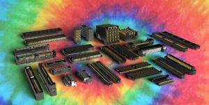
I don't usually look to the Grateful Dead to summarize trends in the electronics industry, but this song title does reflect the last few years in the world of connector raw material costs and availability. For that matter, it pretty much summarizes the entire world for the past 3-4 years. Ron Bishop, the President of Bishop and Associates, and the Bishop team are good, long-time friends of Samtec. So, to put these events in perspective, I talked to Ron about what's going on in the connector … [Read more...]
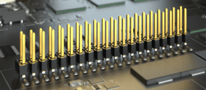
Practical Guidelines To Achieve Quality Connector Solder Joints: Part One
Many factors affect the quality and performance of a connector: pin material, the quality of the stamping, the quality of and choice of surface finish, and the tolerances on the plastic insulator, just to name a few. Beyond the connector, another factor that is crucial to the performance of the connector on the printed circuit board is the quality of the solder joints. This is the first in a series of three blogs, which are interviews with David Decker, the Manager of Samtec … [Read more...]
Connector Plating FAQs: Normal Force, Cycles, Temperature, and Other Essentials
Plating affects the life and quality of the connector system, including corrosion resistance, conductivity, solderability, and of course, cost. This is part two of a discussion with Phil Eckert, Samtec’s Quality Engineering Manager, and Matt Brown, Principal Engineer, about all things pertaining to connector plating. Here’s a link to part one. These blogs, and the upcoming ones in this series, answer connector plating questions that Samtec Quality and Processing experts are frequently asked. … [Read more...]
Connector Plating FAQs: Practical Advice About What Works and What Doesn’t (Part 1)
Like most electronic components, the quality of countless subcomponents and processes directly affects the quality and performance of the finished product. With PCB-level connectors, those factors include pin material, type of plastic, the quality of the molded plastic bodies, coplanarity of the tails, the quality of the surface finish (plating), choosing the correct connector plating, the manufacturing/assembly process (putting the pins in the plastic), and packaging, among others. … [Read more...]
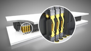
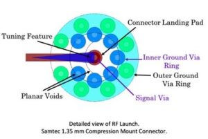
Maximizing RF Launch Performance: The Impact Of GND Vias
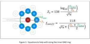
(This is the third in a series of blogs, from Sandeep Sankararaman, Samtec’s Principal RF and Signal Integrity Engineer, discussing design strategies for high-bandwidth RF launches. The first is entitled “What Is An RF Connector Launch?” The second is "Via Stubs: Practical Strategies To Mitigate Return Loss.") A wide bandwidth RF launch requires a good ground ring structure around the signal via to maintain the impedance while the signal travels down the via. Figure 1 shows the ground ring … [Read more...]
Via Stubs: Practical Strategies To Mitigate Return Loss
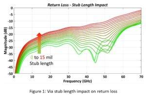
(This is the second in a series of blogs, from Sandeep Sankararaman, Samtec’s Principal RF and Signal Integrity Engineer, discussing design strategies for high-bandwidth RF launches. The first is entitled "What Is An RF Connector Launch?" The third is "Maximizing RF Launch Performance: The Impact of GND Vias." coming next week, discusses GND rings.) When using a through via to transition to an internal layer, there is a stub created by the part of the via that extends below the transition … [Read more...]
What is an RF Launch?
As signal speeds increase, each part of the signal path getting to and from the device needs to work to higher frequencies. Strategies that worked in the past no longer suffice and cheaper connectors no longer make the cut. Cable lengths and trace lengths need to get shorter to reduce losses. This makes intuitive sense. However, what needs to be done with connectors to get them to perform better is not as straightforward. The selection and implementation of RF PCB … [Read more...]
- « Previous Page
- 1
- …
- 5
- 6
- 7
- 8
- 9
- …
- 40
- Next Page »